TIDUF05 August   2022


  1.   Description
  2.   Resources
  3.   Features
  4.   Applications
  5.   5
  6. 1System Description
    1. 1.1 Key System Specifications
  7. 2System Overview
    1. 2.1 Block Diagram
    2. 2.2 Design Considerations
      1. 2.2.1 PCB and Form Factor
      2. 2.2.2 Power Supply Design
        1. 2.2.2.1 POC Filter
        2. 2.2.2.2 Power Supply Considerations
          1. 2.2.2.2.1 Choosing External Components
          2. 2.2.2.2.2 Choosing the Buck 1 Inductor
          3. 2.2.2.2.3 Choosing the Buck 2 and Buck 3 Inductors
        3. 2.2.2.3 Functional Safety
    3. 2.3 Highlighted Products
      1. 2.3.1 AR0820 Imager
      2. 2.3.2 DS90UB953-Q1
      3. 2.3.3 TPS650330-Q1
    4. 2.4 System Design Theory
  8. 3Hardware, Testing Requirements, and Test Results
    1. 3.1 Hardware Requirements
      1. 3.1.1 Hardware Setup
      2. 3.1.2 FPD-Link III I2C Initialization
      3. 3.1.3 AR0820 Initialization
    2. 3.2 Test Setup
      1. 3.2.1 Power Supplies Start Up
      2. 3.2.2 Camera Functionality
    3. 3.3 Test Results
      1. 3.3.1 Power Supplies Start-Up
      2. 3.3.2 Power Supply Start-Up—1.8-V Rail and PDB
      3. 3.3.3 Power Supply Voltage Ripple
      4. 3.3.4 Power Supply Load Currents
      5. 3.3.5 Video Output
  9. 4Design and Documentation Support
    1. 4.1 Design Files
      1. 4.1.1 Schematics
      2. 4.1.2 Bill of Materials
      3. 4.1.3 PCB Layout Recommendations
        1. 4.1.3.1 Layout Prints
        2. 4.1.3.2 PMIC Layout Recommendations
        3. 4.1.3.3 Serializer Layout Recommendations
        4. 4.1.3.4 Imager Layout Recommendations
        5. 4.1.3.5 PCB Layer Stackup Recommendations
      4. 4.1.4 Altium Project
      5. 4.1.5 Gerber Files
  10. 5Documentation Support
  11. 6Support Resources
  12. 7Trademarks

PMIC Layout Recommendations

The PMIC portion of the layout requires careful consideration to minimize both PCB area and noise. As EMI is a critical concern in automotive systems, the TPS650330-Q1 device includes a spread spectrum feature to reduce conducted and radiated emissions, allowing more flexibility with placement and layout for space-constrained applications. However, it is still recommended to follow as many best practices as possible. This includes minimizing the area traveled by switching currents between buck regulator input capacitor, inductor, and output capacitor with tight component placement and minimal return path to the PMIC thermal pad. Figure 4-1 shows an example of this for buck 1 and buck 3.

For the LDO, separation of input and output capacitor ground planes will reduce noise coupling from the switching rails to the sensitive 2.8-V analog rail. To further reduce noise coupling, the dedicated AGND pin of the PMIC is connected to the ground plane on an internal layer with a via, rather than directly to the noisier thermal pad on the top layer.
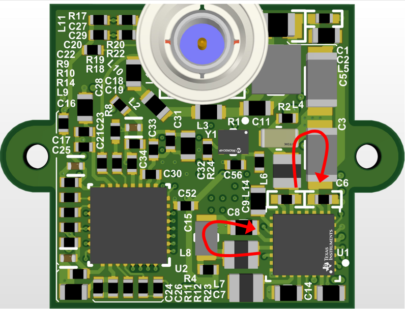
GUID-20220421-SS0I-JLFR-MJPP-VT6NXPM7P9TQ-low.pngFigure 4-1 PMIC PCB Layout