TIDUF05 August 2022
- Description
- Resources
- Features
- Applications
- 5
- 1System Description
- 2System Overview
- 3Hardware, Testing Requirements, and Test Results
- 4Design and Documentation Support
- 5Documentation Support
- 6Support Resources
- 7Trademarks
4.1.3.3 Serializer Layout Recommendations
Decoupling capacitors must be located very close to the supply pin on the serializer. Again, this requires consideration of the path of the supply current and the return current. Keeping the loop area of this connection small reduces the parasitic inductance associated with the connection of the capacitor. Due to space constraints, ideal placement is not always possible. For decoupling capacitors placed on the opposite layer of the serializer, minimize the return path to the serializer thermal pad. Place smaller value capacitors that provide higher frequency decoupling closest to the device.
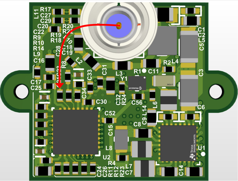
For this application, a single-ended impedance of 50 Ω is required for the coax interconnect. Anti-pads are implemented in the ground plane under critical components such as the DOUT AC coupling capacitors to minimize impedance mismatch. Keep the coax connection to the serializer short. Figure 4-1 shows the routing of the high-speed serial line, highlighted by the redline. The total length of the red line is about ½ inch.
Lastly, minimize crosstalk between high-speed data lines by ensuring the high-speed data routing on adjacent layers do not overlap. If they must overlap due to space constraints, place a ground layer between the two routing layers as a buffer. Keep high speed trace vias to a minimum. The vias must ideally be two or fewer to reduce stubs that cause reflections.
 Figure 4-2 High-Speed Trace Routing