TIDT196 September 2020 – MONTH
4.2 Output Voltage Ripple
The following figures show the output voltage ripple of the converter as measured at the terminals across a 0.1µF capacitor.
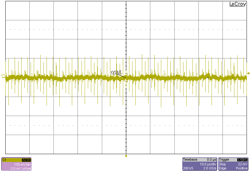 Figure 4-5 Ripple, 8-V Input, 615-W Load
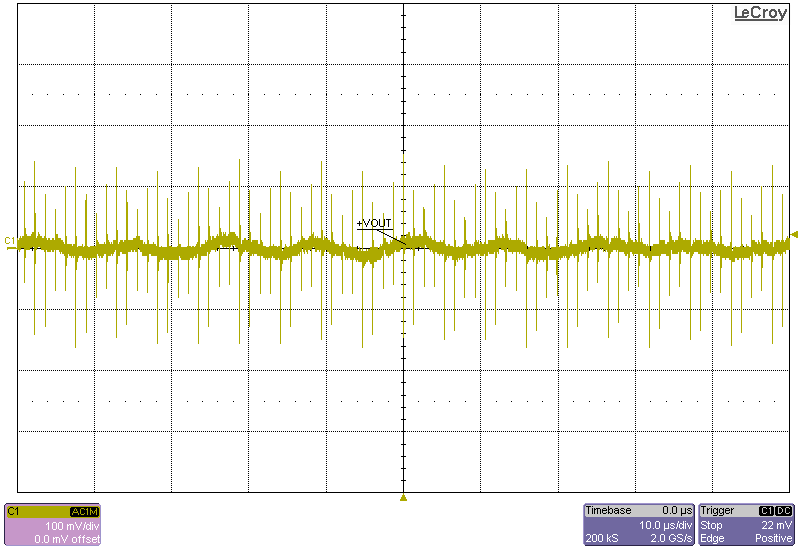 Figure 4-7 Ripple, 12-V Input, 1230-W Load
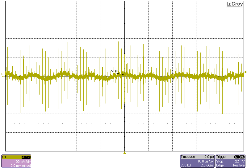 Figure 4-9 Ripple, 18-V Input, 1230-W Load
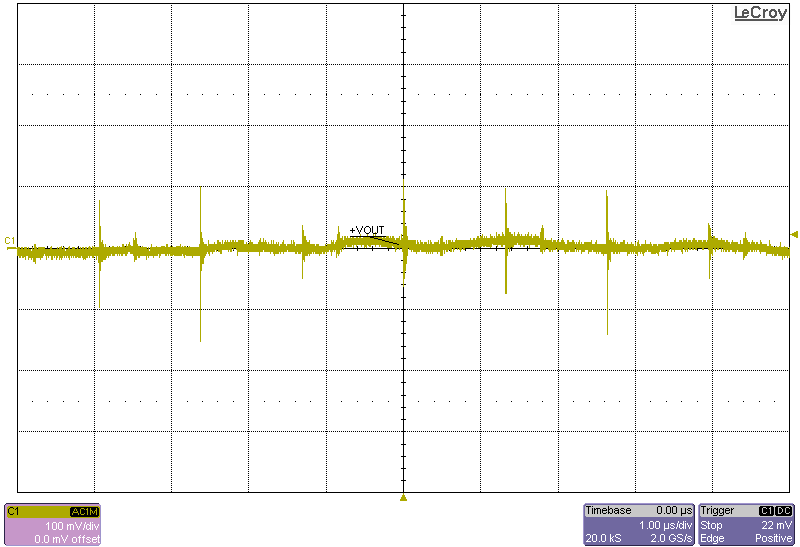 Figure 4-6 Ripple, 8-V Input, 615-W Load
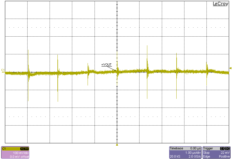 Figure 4-8 Ripple, 12-V Input, 1230-W Load
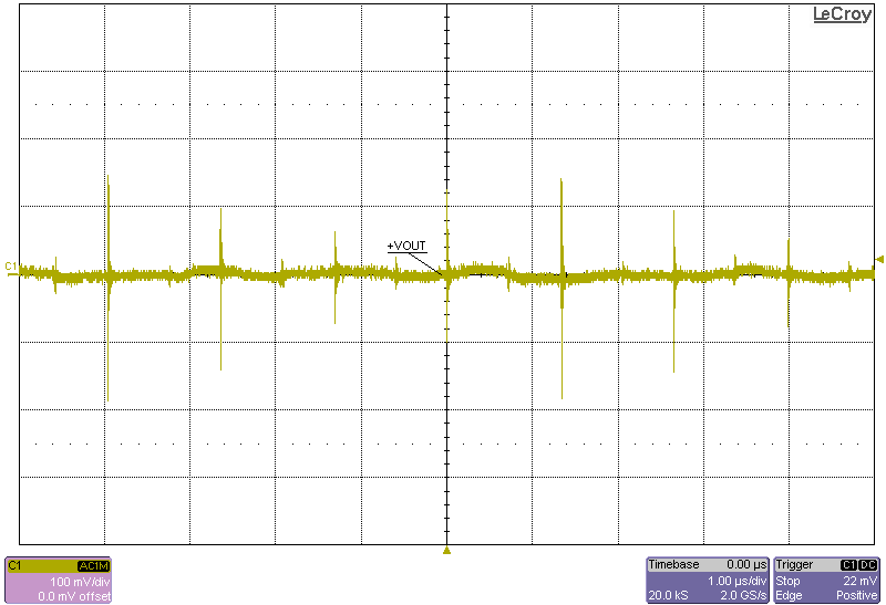 Figure 4-10 Ripple, 18-V Input, 1230-W Load