TIDT196 September 2020 – MONTH
4.1 Switching
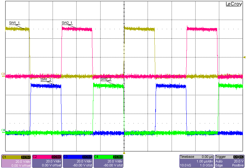
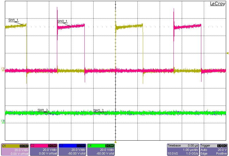
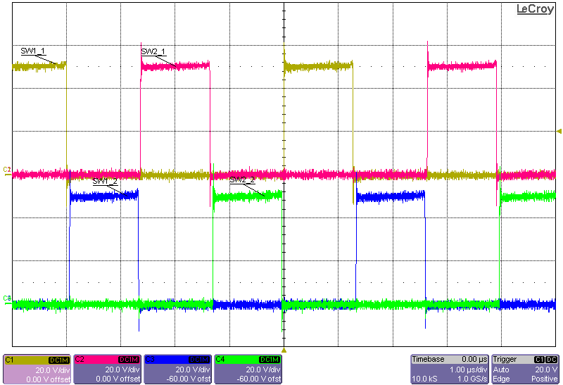
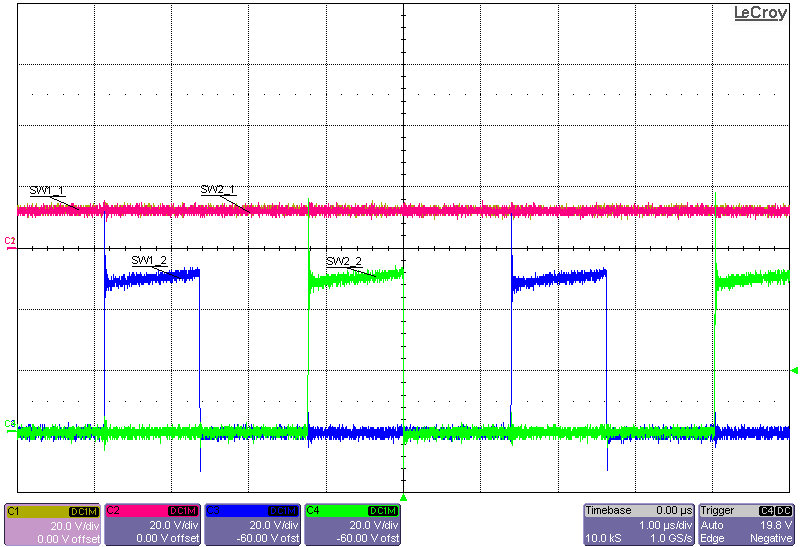
The switching behavior is shown in the following figures.
 Figure 4-1 4-Phase Switching, 12-V Input, 0-W Load
 Figure 4-3 2-Phase Switching, 12-V Input, 1230-W Load
 Figure 4-2 4-Phase Switching, 12-V Input, 1230-W Load
 Figure 4-4 2-Phase Switching, 12-V Input, 1230-W Load