SWRU585 November 2021
- Trademarks
- 1Getting Started
- 2Hardware
- 3PCB Storage and Handling Recommendations
- 4IWR6843LEVM Antenna
-
5Hardware Details
- 5.1 Switch Settings
- 5.2 LEDs
- 5.3 Connectors
- 5.4 USB Connector
- 5.5 DCA1000 HD Connector
- 5.6 MMWAVEICBOOST HD Connector
- 5.7 CANFD Connector
- 5.8 I2C Connections
- 5.9 EEPROM
- 5.10 Default I2C Address
- 5.11 Modular Mode
- 5.12 Flashing the Board
- 5.13 DCA1000EVM Mode
- 5.14 MMWAVEICBOOST Mode
- 5.15 Raw ADC Data Capture Using MMWAVEICBOOST and DCA1000 EVMs
- 5.16 Muxing Scheme
- 6Software, Development Tools, and Example Code
- 7TI E2E Community
- 8References
5.1 Switch Settings
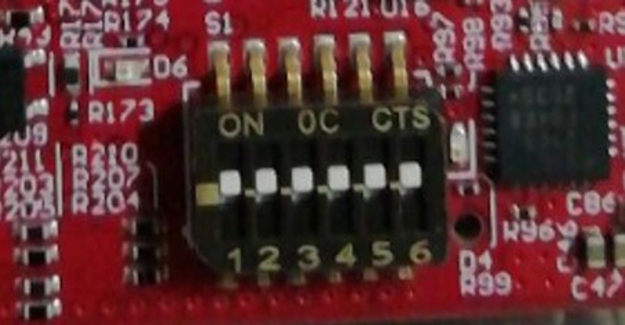
Figure 5-1 shows the part designators and positions of the switches on the IWR6843LEVM.
 Figure 5-1 Part Designators and Positions
of the Switches on the IWR6843LEVM
Figure 5-1 Part Designators and Positions
of the Switches on the IWR6843LEVMTable 5-1 Switches, Buttons and
Muxes
| Reference Designator | Switch On | Switch Off |
|---|---|---|
| S1.1 | SOP2 pulled up | SOP2 pulled down |
| S1.2 | SOP1 pulled up | SOP1 pulled down |
| S1.3 | SOP0 pulled up | SOP0 pulled down |
| S1.4 | Muxes to CAN connector J3, J4 | Muxes to serial peripheral interface (SPI) on 60 pin connector, J1, J6 |
| S1.5 | Muxes USER UART to 60 pin header J1 | Muxes USER UART to USB connector J5 |
| S1.6 | - | - |
| S2 | Reset switch | |
| S3 | GPIO1 toggle switch | |