SWRU585 November 2021
- Trademarks
- 1Getting Started
- 2Hardware
- 3PCB Storage and Handling Recommendations
- 4IWR6843LEVM Antenna
-
5Hardware Details
- 5.1 Switch Settings
- 5.2 LEDs
- 5.3 Connectors
- 5.4 USB Connector
- 5.5 DCA1000 HD Connector
- 5.6 MMWAVEICBOOST HD Connector
- 5.7 CANFD Connector
- 5.8 I2C Connections
- 5.9 EEPROM
- 5.10 Default I2C Address
- 5.11 Modular Mode
- 5.12 Flashing the Board
- 5.13 DCA1000EVM Mode
- 5.14 MMWAVEICBOOST Mode
- 5.15 Raw ADC Data Capture Using MMWAVEICBOOST and DCA1000 EVMs
- 5.16 Muxing Scheme
- 6Software, Development Tools, and Example Code
- 7TI E2E Community
- 8References
5.14 MMWAVEICBOOST Mode
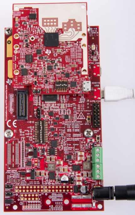
In this mode the boards are setup as shown in Figure 5-10, UART is routed to the 60 pin connector to the XDS110 USB. This mode enables access to debugging tools available on the MMWAVEICBOOST such as the JTAG, RAW ADC capture through MMWAVEICBOOST camera-mount option, CAN, Launchpad connector, and so forth.
Note: In MMWAVEICBOOST mode, the
IWR6843LEVM is mounted on the MMWAVEICBOOST and the SOP mode is set by the
MMWAVEICBOOST.
More on the mmWAVEICBOOST, setup and features it provides can be found in the MMWAVEICBOOST section of MMWAVEICBOOST EVM userguide.
 Figure 5-10 MMWAVEICBOOST Mode