SPRUJ74 January   2023


  1.   Trademarks
  2. 1Introduction
    1. 1.1 Key Features
    2. 1.2 Thermal Compliance
    3. 1.3 EMC, EMI, and ESD Compliance
  3. 2QP-ENET Board Identification and Installation
    1. 2.1 QP-ENET Board Component Identification
    2. 2.2 Interfacing QP-ENET Expansion Board with J784S4XG01EVM Board
      1. 2.2.1 Detailed Board Assembly Procedure (J784S4XG01EVM)
  4. 3QP-ENET Expansion Board Hardware Architecture
    1. 3.1 QP-ENET Expansion Board Hardware Top Level Diagram
    2. 3.2 Expansion Connectors
    3. 3.3 Board ID EEPROM
    4. 3.4 Ethernet Interface
      1. 3.4.1 Quad Port SGMII PHY Default Configuration
      2. 3.4.2 SGMII Clocking Scheme
        1. 3.4.2.1 Main Clock
        2. 3.4.2.2 Optional Clock
      3. 3.4.3 Ethernet Port LED Indication
      4. 3.4.4 Reset and Power-down Signals
  5. 4Revision History
  6.   A Appendix
    1.     A.1 Appendix – I (Interface Mapping)
    2.     A.2 Appendix – II (QP-ENET Board GPIO Mapping)

Interfacing QP-ENET Expansion Board with J784S4XG01EVM Board

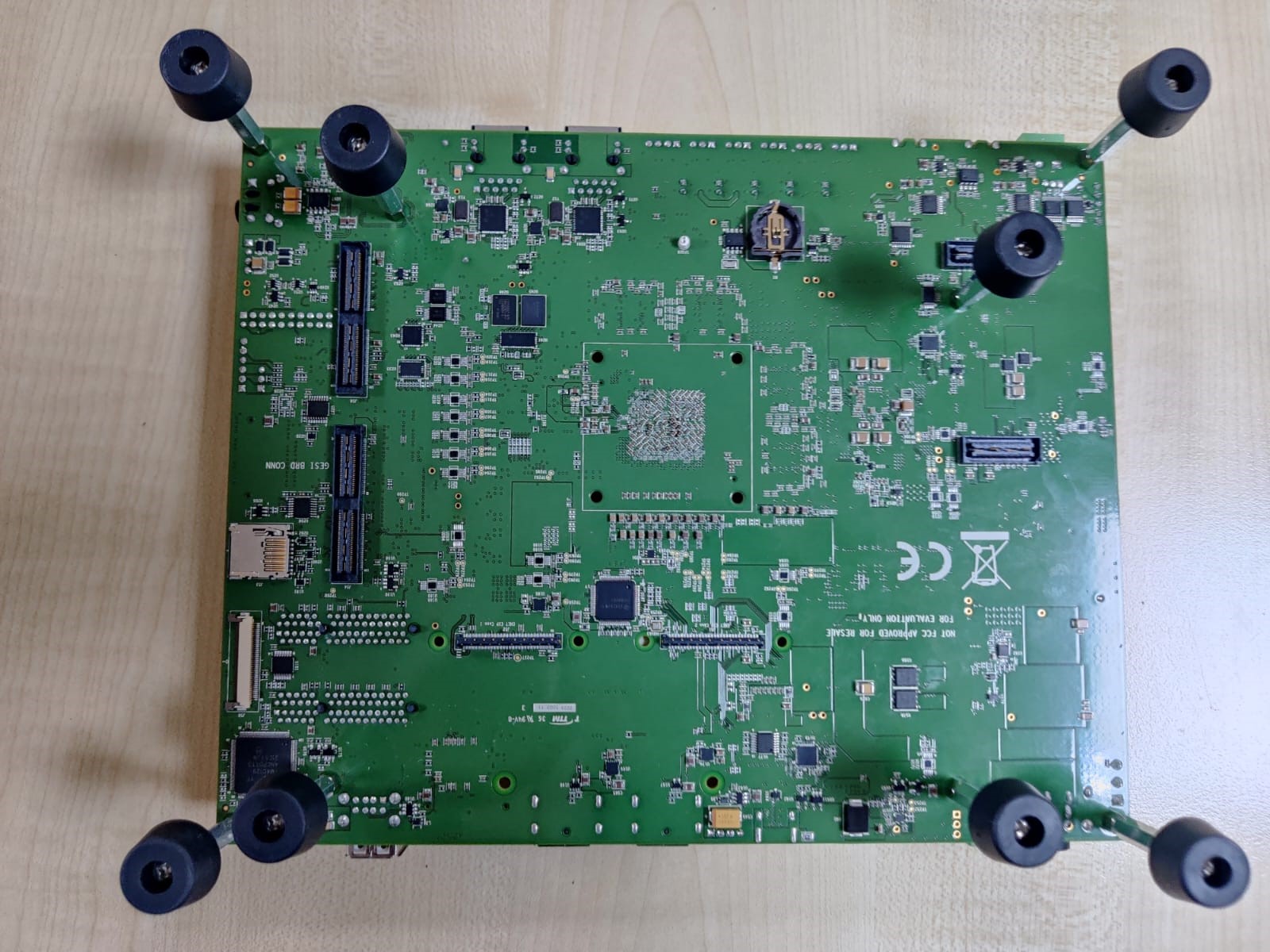
QP-ENET Expansion boards shall be interfaced with Jacinto7 J784S4XG01EVM in bottom mating configurations. The images below show the J7AHP EVM board connectors J51 and J52, which mate with the QP-ENET board as an example, with expansion connectors J3 on the QP-ENET mated to the SGMII Expansion connectors on the J7AHP EVM. It is valid to support/install on only one QP-ENET board, and in either location.
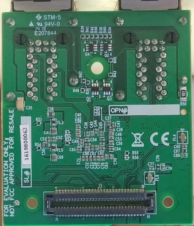
GUID-26F11822-3EC0-4463-9B74-E790874078BB-low.jpg Figure 2-2 QP-ENET Expansion Board Bottom Side
GUID-3332434A-B97D-459B-8032-25E802BBE4D7-low.jpg Figure 2-3 Q/SGMII Expansion Connector on J784S4XG01EVM Bottom Side