SPRUJ74 January 2023
3.4.2.2 Optional Clock
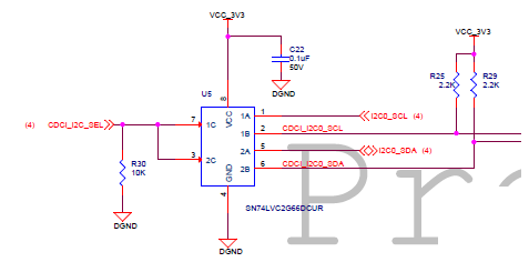
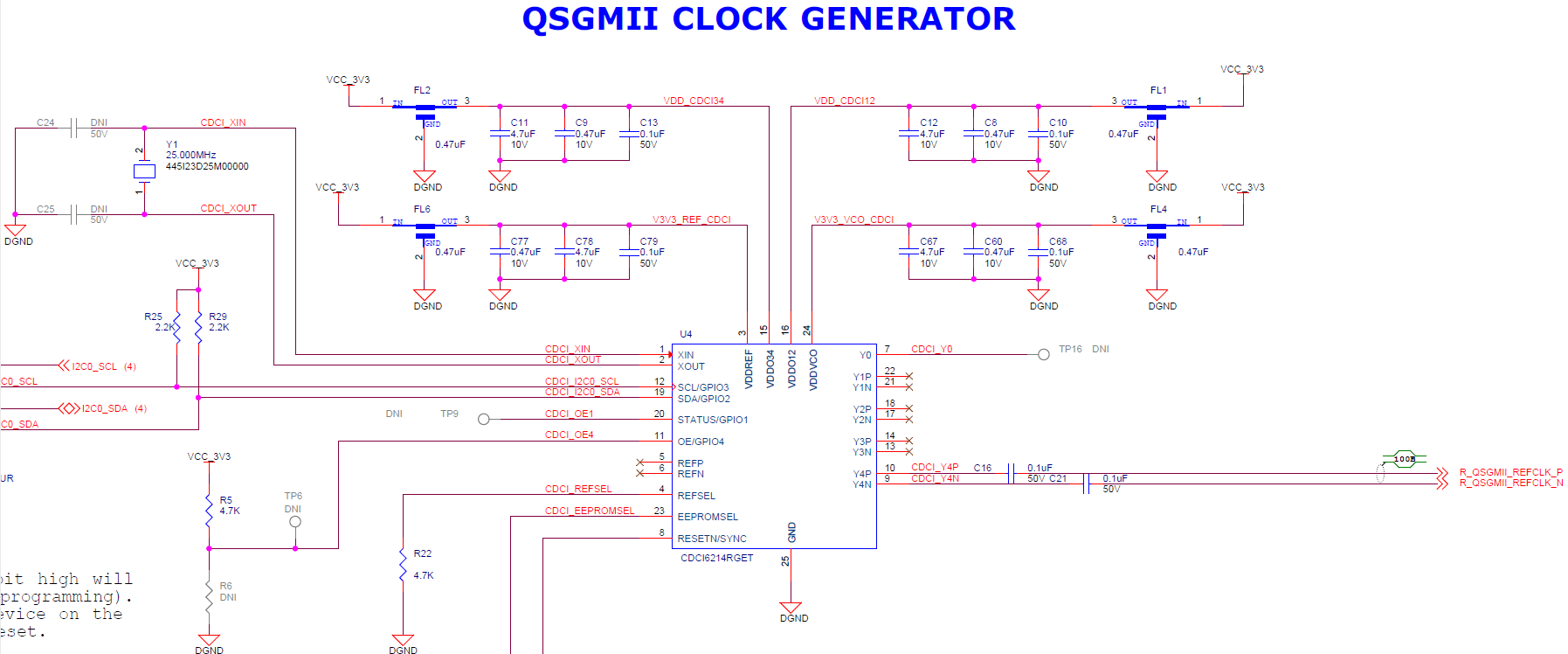
Optionally, the reference clock can be supplied by the SERDES clock generator Mfr. Part Number# CDCI6214RGET located on QP-ENET Board, which can be configured by I2C0 of the J7 SOC. The I2C address of this clock generator is 0x77, and this address conflicts with the CDCI Chip on EVM Boards. An I2C switch on the Quad port Ethernet Expansion Board is used to remove the address conflict by connecting any one of the clock generators.
 Figure 3-4 Clock Source I2C MUX
 Figure 3-5 QP-ENET Optional Clock Source
Setting the CDCI_I2C_SEL IO EXP bit high will connect the I2C bus to CDCI (for programming) on the Quad Port Ethernet Expansion Board. During this time, the CDCI device on the EVM boards should be in reset mode. Also, there are resistor options provided that must be adjusted to reflect any change in source clock selection; this is given in the following images.
 Figure 3-6 SGMII PHY Clock Input Source Path Selection
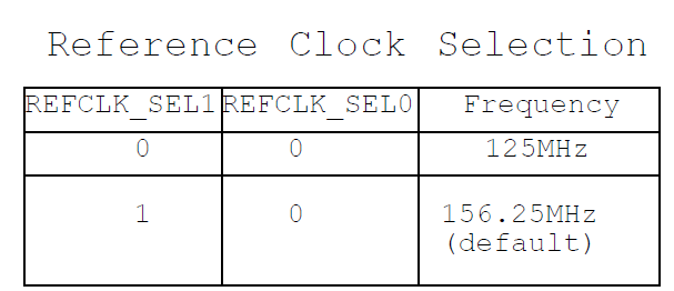
 Figure 3-7 SGMII PHY Clock Configuration