SPRUJ74 January   2023


  1.   Trademarks
  2. 1Introduction
    1. 1.1 Key Features
    2. 1.2 Thermal Compliance
    3. 1.3 EMC, EMI, and ESD Compliance
  3. 2QP-ENET Board Identification and Installation
    1. 2.1 QP-ENET Board Component Identification
    2. 2.2 Interfacing QP-ENET Expansion Board with J784S4XG01EVM Board
      1. 2.2.1 Detailed Board Assembly Procedure (J784S4XG01EVM)
  4. 3QP-ENET Expansion Board Hardware Architecture
    1. 3.1 QP-ENET Expansion Board Hardware Top Level Diagram
    2. 3.2 Expansion Connectors
    3. 3.3 Board ID EEPROM
    4. 3.4 Ethernet Interface
      1. 3.4.1 Quad Port SGMII PHY Default Configuration
      2. 3.4.2 SGMII Clocking Scheme
        1. 3.4.2.1 Main Clock
        2. 3.4.2.2 Optional Clock
      3. 3.4.3 Ethernet Port LED Indication
      4. 3.4.4 Reset and Power-down Signals
  5. 4Revision History
  6.   A Appendix
    1.     A.1 Appendix – I (Interface Mapping)
    2.     A.2 Appendix – II (QP-ENET Board GPIO Mapping)

Main Clock

The reference clock to the PHY is generated from TI’s Clock Generator Mfr. Part Number# CDCI6214RGET, which is placed on the J7AHP EVM Board. Clock inputs are AC coupled and LVDS compliant. The clock generator can be configured by I2C0 of the J7AHP SoC. The I2C address of this clock generator is 0x77.
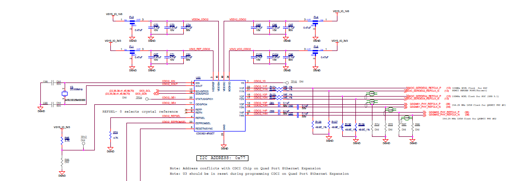
GUID-5728E9A9-6A20-495D-BA3A-770C34807F76-low.png Figure 3-3 Default Clock Source on J7AHP EVM Board