SPRACP6 December 2019 TMS320F2800132 , TMS320F2800133 , TMS320F2800135 , TMS320F2800137 , TMS320F2800152-Q1 , TMS320F2800153-Q1 , TMS320F2800154-Q1 , TMS320F2800155 , TMS320F2800155-Q1 , TMS320F2800156-Q1 , TMS320F2800157 , TMS320F2800157-Q1 , TMS320F280021 , TMS320F280021-Q1 , TMS320F280023 , TMS320F280023-Q1 , TMS320F280023C , TMS320F280025 , TMS320F280025-Q1 , TMS320F280025C , TMS320F280025C-Q1 , TMS320F280040-Q1 , TMS320F280040C-Q1 , TMS320F280041 , TMS320F280041-Q1 , TMS320F280041C , TMS320F280041C-Q1 , TMS320F280045 , TMS320F280048-Q1 , TMS320F280048C-Q1 , TMS320F280049 , TMS320F280049-Q1 , TMS320F280049C , TMS320F280049C-Q1
- How to Maximize GPIO Usage in C2000 Devices
3 cJTAG Option
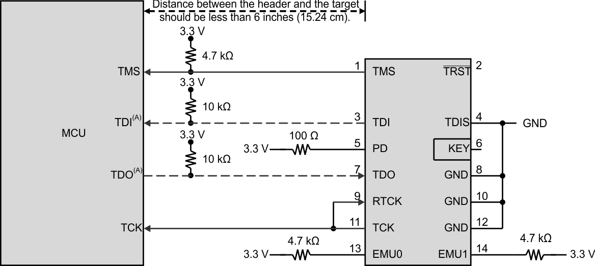
Contrary to previous devices, the F28004x device supports cJTAG connection as shown in Figure 1. JTAG port has four dedicated pins: TMS, TDI, TDO, and TCK, while cJTAG port is a compact JTAG interface requiring only two pins (TMS and TCK). Thus, the traditional GPIO35 (TDI) and GPIO37 (TDO) pins can be muxed as other peripheral functions.
Compared to JTAG, cJTAG provides lower performance because it uses only two pins: TMS and TCK. Basically, TDI, TDO and TMS functionality is implemented on single pin, TMS. The maximum supported clock frequency on TCK is 15 MHz for JTAG, and for cJTAG, it decreases to 10 MHz. Note that in order to use cJTAG, a supported debug probe is required, such as XDS100V3, XDS110, XDS200, and so forth.
