SNLA267A March 2019 – June 2019 DS90UB953-Q1 , DS90UB954-Q1 , DS90UB960-Q1
-
How to Design a FPD-Link III System Using DS90UB953-Q1 and DS90UB954-Q1
- Trademarks
- 1 Overview
- 2 Basic Design Rules
- 3 Designing the Link Between SER and DES
- 4 Designing Link Between SER and Image Sensor
- 5 Designing Link Between DES and ISP
- 6 Hardware Design
- 7
Appendix
- 7.1
Scripts
- 7.1.1 BIST Script
- 7.1.2 Example Sensor Initialization Script
- 7.1.3 CSI Enable and Port Forwarding Script
- 7.1.4 Enabling CMLOUT FPD3 RX Port 0 on 954
- 7.1.5 Remote Enabled SER GPIO Toggle Script
- 7.1.6 Local SER GPIO Toggle Script
- 7.1.7 Internal FrameSync on 953 GPIO1
- 7.1.8 External FrameSync on 953 GPIO0
- 7.1.9 SER GPIOs as Inputs and Output to DES GPIO
- 7.1.10 Pattern Generation on the 953 Script
- 7.1.11 Pattern Generation on the 954 Script
- 7.1.12 Monitor Errors for Predetermined Time Script
- 7.1.13 954 and 953 CSI Register Check Script
- 7.1.14 Time Till Lock Script on 953
- 7.2 Acknowledgments
- 7.1
Scripts
- Revision History
2.1.1.1 Synchronous Mode
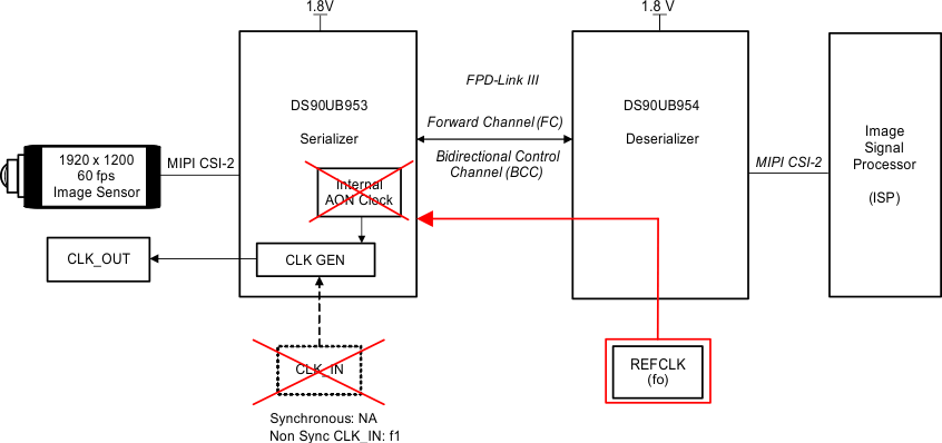
 Figure 4. Illustration of Synchronous Clocking
 The first mode, synchronous, is an internally generated clock. This clock reference is extracted from back channel on the bidirectional communications link, and the internal PLLs take the extracted signal to generate the required clocks. This allows multiple cameras within a system to operate in the same clock domain and allows more space on the PCB. As shown in Figure 4, REFCLK (f0) is input signal on the deserializer that is required for precise frequency operation. Refer to the REFCLK section in the 954 data sheet for more information. The RECLK specifications for the 953 states that REFCLK must range from 24 to 26 MHz, and this signal sends two bits across the back channel: high and low. As a result, multiply the REFCLK frequency by two when calculating the BC and FC rate. This is summarized in Table 5.