SNLA267A March 2019 – June 2019 DS90UB953-Q1 , DS90UB954-Q1 , DS90UB960-Q1
-
How to Design a FPD-Link III System Using DS90UB953-Q1 and DS90UB954-Q1
- Trademarks
- 1 Overview
- 2 Basic Design Rules
- 3 Designing the Link Between SER and DES
- 4 Designing Link Between SER and Image Sensor
- 5 Designing Link Between DES and ISP
- 6 Hardware Design
- 7
Appendix
- 7.1
Scripts
- 7.1.1 BIST Script
- 7.1.2 Example Sensor Initialization Script
- 7.1.3 CSI Enable and Port Forwarding Script
- 7.1.4 Enabling CMLOUT FPD3 RX Port 0 on 954
- 7.1.5 Remote Enabled SER GPIO Toggle Script
- 7.1.6 Local SER GPIO Toggle Script
- 7.1.7 Internal FrameSync on 953 GPIO1
- 7.1.8 External FrameSync on 953 GPIO0
- 7.1.9 SER GPIOs as Inputs and Output to DES GPIO
- 7.1.10 Pattern Generation on the 953 Script
- 7.1.11 Pattern Generation on the 954 Script
- 7.1.12 Monitor Errors for Predetermined Time Script
- 7.1.13 954 and 953 CSI Register Check Script
- 7.1.14 Time Till Lock Script on 953
- 7.2 Acknowledgments
- 7.1
Scripts
- Revision History
5.1.2 Internal and External Frame Sync Configuration
TI recommends that frame sync is always sent from the deserializer using Internal or External Frame Sync. In multi-camera systems, it is important that every frame sync is sent to each camera at the same time. If the system uses the SER GPIOs to send a frame sync signal to the Image Sensor, the SER GPIOs must always be remote enabled whether the frame sync is internally or externally generated.
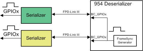
 Figure 17. Block Diagram of Internally Generated Frame Sync
 As shown in Figure 17, internally generated frame sync signals come from an internal block of the 954. Defining a GPIO for an internal frame sync generator can be accessed in any BC_GPIO_CTLx register (0x6E-0x6F).
Configuring the internal frame sync mode is done in the FS_CTL register with an address of 0x18. Enabling the internal FrameSync mode is done by setting the first bit of the FS_CTL register (0x18 [0]) to a value of 1, which is the FS_GEN_ENABLE control. The last four bits of the FS_CTL register, FS_MODE field (0x18 [7:4]), controls the clock source used for the FrameSync generation. The second bit in FS_CTL—the FS_GEN_MODE field (0x18 [1])—configures whether the duty cycle of the FrameSync is 50/50 or whether the high and low periods are controlled separately.
The FrameSync high and low periods are controlled by the FS_HIGH_TIME_x and FS_LOW_TIME_x (0x19–0x1C) registers. For more information regarding how to program high and low time frame sync, refer to the 954 data sheet. The resolution of the FrameSync generator clock (FS_CLK_PD) is derived from the back channel frame period. The frame period can be found in the first 3 bits of the BC_CONFIG register—the BC FREQ SELECT (0x58 [2:0]). For 50-Mbps back channel operation, the frame period is 600 ns (30 bits × 20 ns/bit).
An example on how to enable the Frame sync this way is shown in Section 5.1.1.
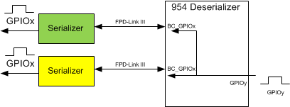
 Figure 18. Block Diagram of Externally Generated Frame Sync
 In External FrameSync mode, an external signal inputs to the DS90UB954-Q1 through one of the GPIO pins on the device. As shown in Figure 18, the external FrameSync signal may be propagated to one or more of the attached FPD3 serializers through a GPIO signal in the back channel. The expected skew timing for external FrameSynch mode is on the order of one back channel frame period.
Enabling the external FrameSync mode is done by setting the last 4 bits of the FS_CTL register (0x18 [7:4]) that indicates the FS_MODE control. The value should be between 0x8 (GPIO0 pin) to 0xF (GPIO7 pin). Set FS_GEN_ENABLE to 0 for this mode.
To send the FrameSync signal on a port’s BC_GPIOx signal, the BC_GPIO_CTL0 (0x6E) or BC_GPIO_CTL1 (0x6F) register should be programmed for that port to select the FrameSync signal.