SNLA267A March 2019 – June 2019 DS90UB953-Q1 , DS90UB954-Q1 , DS90UB960-Q1
-
How to Design a FPD-Link III System Using DS90UB953-Q1 and DS90UB954-Q1
- Trademarks
- 1 Overview
- 2 Basic Design Rules
- 3 Designing the Link Between SER and DES
- 4 Designing Link Between SER and Image Sensor
- 5 Designing Link Between DES and ISP
- 6 Hardware Design
- 7
Appendix
- 7.1
Scripts
- 7.1.1 BIST Script
- 7.1.2 Example Sensor Initialization Script
- 7.1.3 CSI Enable and Port Forwarding Script
- 7.1.4 Enabling CMLOUT FPD3 RX Port 0 on 954
- 7.1.5 Remote Enabled SER GPIO Toggle Script
- 7.1.6 Local SER GPIO Toggle Script
- 7.1.7 Internal FrameSync on 953 GPIO1
- 7.1.8 External FrameSync on 953 GPIO0
- 7.1.9 SER GPIOs as Inputs and Output to DES GPIO
- 7.1.10 Pattern Generation on the 953 Script
- 7.1.11 Pattern Generation on the 954 Script
- 7.1.12 Monitor Errors for Predetermined Time Script
- 7.1.13 954 and 953 CSI Register Check Script
- 7.1.14 Time Till Lock Script on 953
- 7.2 Acknowledgments
- 7.1
Scripts
- Revision History
4.2 CLKOUT
 Figure 12. Clocking System Diagram
 The 953 clock outline is intended as a reference clock for the image sensor. Note that the CLK_OUT/IDX pin (19) also assigns the I2C device ID on power up. See Section 2.1 for information. After power up, the clock out frequency is defined by Equation 5.
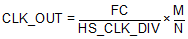
- FC is the forward channel data rate,
- M, HS_CLK_DIV, and N are parameters set by the CLKOUT control registers 0x06 and 0x07 on the 953.
where
For more information for calculating FC, see Section 2.1.1.
The PLL that generates CLK_OUT is a digital PLL that will have very low jitter if the ratio N/M is an integer. However, if N/M is not an integer, then the jitter on the signal will be approximately equal to HS_CLK_DIV/FC. As a result, if it is not possible to have an integer ratio of N/M, it is best to select a small value for HS_CLK_DIV.
If a particular frequency is required, for a system (for example, 37.125 MHz), then using values of M=0x09, N=0xF2, and HS_CLK_DIV=4 will result in an output frequency of 37.19 MHz and a frequency error of 0.175% with jitter of about 1 ns. Alternately, you could use M=0x01, N=0x1E, and HS_CLK_DIV=4 and get an output frequency of 37.037 MHz and a frequency error of 0.24% with much less jitter. A third alternative would be to use the M=0x01, N=0x1E, and HS_CLK_DIV=4, but rather than using a 25-MHz clock frequency for the DS90UB954-Q1 reference, use a frequency of 25.059 MHz for the DS90UB953-Q1 to get both a low jitter and low frequency error.