SNAU309 October   2025 LMK3H2108


  1.   1
  2.   Description
  3.   Features
  4.   Applications
  5.   5
  6. 1Evaluation Module Overview
    1. 1.1 Introduction
    2. 1.2 Kit Contents
    3. 1.3 Specification
    4. 1.4 Device Information
  7. 2Hardware
    1. 2.1 EVM Quick Start
      1. 2.1.1 Hardware Setup
      2. 2.1.2 Software Setup
    2. 2.2 EVM Configuration
      1. 2.2.1 Device Operational Modes
      2. 2.2.2 Power Supply
      3. 2.2.3 Logic Inputs and Outputs
      4. 2.2.4 Configuring the Clock Outputs
      5. 2.2.5 Using the USB Interface Connection
  8. 3Software
    1. 3.1 Software Installation
    2. 3.2 Software Description
      1. 3.2.1 User Controls Page
      2. 3.2.2 Raw Registers Page
      3. 3.2.3 Global Settings Page
      4. 3.2.4 EFUSE Pages Page
      5. 3.2.5 GPIO Page
      6. 3.2.6 FODs Page
      7. 3.2.7 Inputs Page
      8. 3.2.8 OUT0 Page
      9. 3.2.9 OUT1 & OUT2 Page
  9. 4Implementation Results
    1. 4.1 Evaluation Setup
    2. 4.2 Performance Data and Results
  10. 5Hardware Design Files
    1. 5.1 Schematics
    2. 5.2 PCB Layouts
    3. 5.3 Bill of Materials (BOM)
  11. 6Additional Information
    1. 6.1 Trademarks
  12. 7Related Documentation
    1. 7.1 Supplemental Content

Inputs Page

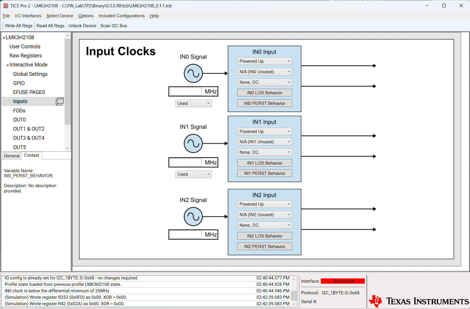
LMK3H2108EVM LMK3H2108 Inputs Page Figure 3-7 LMK3H2108 Inputs Page

The Inputs page allows for modification of the LMK3H2108 input buffers. Each input consists of the following fields:

  • Input frequency: Used solely for calculation purposes on the output pages
  • Power state: Whether the input path is enabled or disabled
  • Input format: Disabled, INx_P LVCMOS, INx_N LVCMOS, or INx Differential
  • Input termination, capable of supporting any input format
  • Loss of signal behavior
  • PCIe Reset (PERST) mode behavior