SNAU271 October 2021
6 Input Clock Selection
The LMK1D1212 can receive either a differential or single-ended clock as input. The default board configuration is for a differential signal at both device inputs. The inputs can be applied through the SMAs, J3, J4 (IN0_P, IN0_N) or J5, J6 (IN1_P, IN1_N). These inputs are AC-coupled to the device. The common-mode voltage is provided by the device on-chip bias generator (VAC_REF) pins.
LMK1D1212: Jumper, J10, can be used to select between the two input clocks. IN0 is selected when J10 connects IN_SEL to GND. IN1 is selected when J10 connects IN_SEL to VDD.
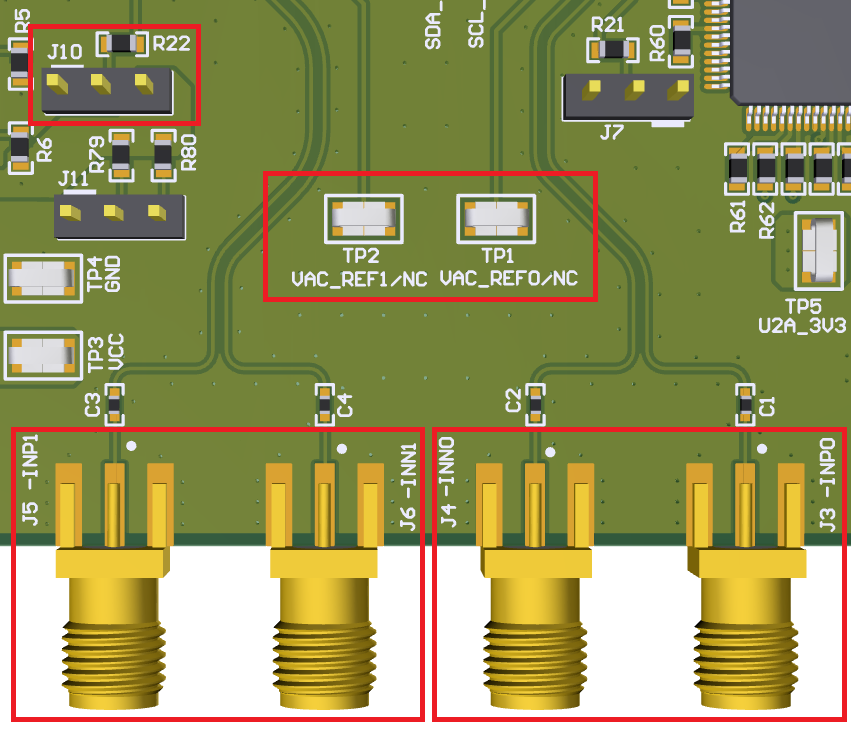 Figure 6-1 Input Clock Selection Layout.