SNAU271 October 2021 LMK1D1212
7 Output Clock
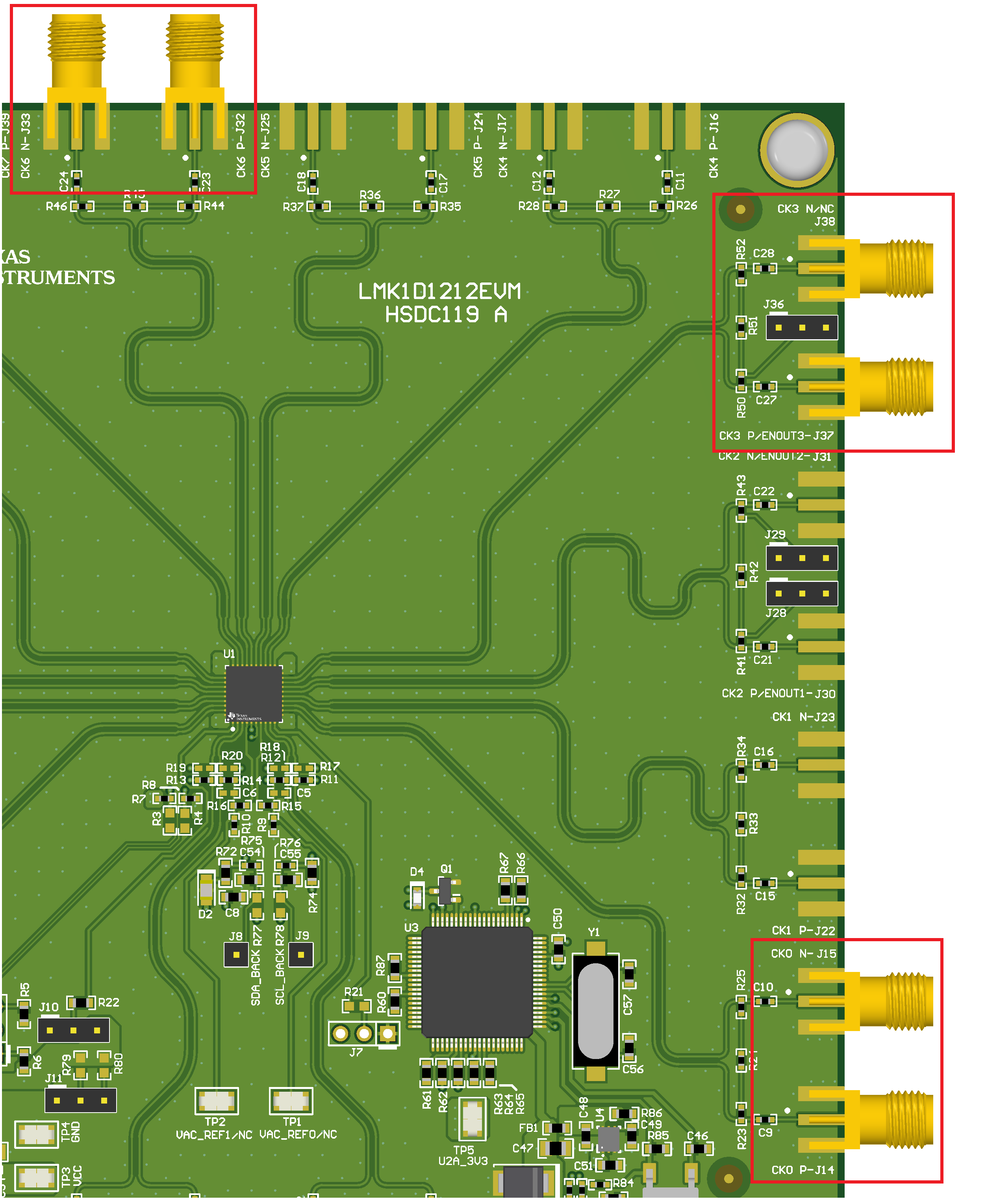
The LMK1D1212 generates up to 12 LVDS outputs. Three outputs (OUT0, OUT3 and OUT6) are available by default on the EVM through the following SMAs: J14, J15 (OUT0_P, OUT0_N), J37, J38 (OUT3_P, OUT3_N), and J32, J33 (OUT6_P, OUT6_N).
The LVDS outputs are AC-coupled to their respective SMAs. Each output pair has the 100-Ω termination on the board already populated: R24 (OUT0), R51 (OUT3), and R45 (OUT6).
 Figure 7-1 Output Clock EVM Layout .