SNAU271 October 2021 LMK1D1212
6.2 Single-Ended Input
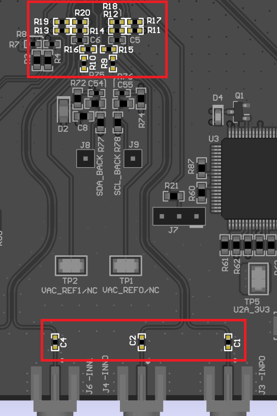
Single-ended input must be configured by replacing or removing passive components on the board. Follow Table 6-1 for proper setup of a single-ended input.
Table 6-1 Single-Ended Configurations by Bias Voltage
| BIAS VOLTAGE TO INx_N (V) | INPUT TO INx_P (V) | INPUT | REMOVE BIASING RESISTOR | REMOVE COMMON-MODE RESISTOR | REPLACE WITH 0-Ω RESISTOR | REPLACE WITH 100-Ω RESISTOR |
|---|---|---|---|---|---|---|
| 0.9 | 1.8 (LVCMOS) | IN0_N | R11 R12 | R15 | C1 | N/A |
IN0_P | C2 | N/A | ||||
| 0.9 | 1.8 (LVCMOS) | IN1_N | R13 R14 | R16 | C3 | N/A |
IN1_P | C4 | N/A | ||||
| 1.25 | 2.5 (LVCMOS) | IN0_N | R12 | R15 | R9 C1, C2 | R17 R18 |
IN0_P | ||||||
| 1.25 | 2.5 (LVCMOS) | IN1_N | R14 | R16 | R10 C3, C4 | R19 R20 |
IN1_P | ||||||
1.65 | 3.3 (LVCMOS) | IN0_N | R12 | R15 | R9 C1, C2 | R17 R18 |
IN0_P | ||||||
| 1.65 | 3.3 (LVCMOS) | IN1_N | R14 | R16 | R10 C3, C4 | R19 R20 |
IN1_P |
 Figure 6-2 Components to Modify for Single-Ended Configuration.