SNAA360 June 2022 ADC32RF54 , ADC32RF55 , AFE7950 , LMX1204
1.1 Cascaded LMX1204 Design
The LMX1204 creates up to four copies of an input signal, including the ability to buffer, multiply, or divide the signal to each of the outputs. This device distributes a single low power clock signal and with minimal added phase noise per stage. This design supports a two-level cascaded implementation creating 16 output clocks for distribution as shown in Figure 1-1.
 Figure 1-1 Simple Block Diagram of
Cascaded LMX1204 Design
Figure 1-1 Simple Block Diagram of
Cascaded LMX1204 DesignThe purpose of this design is to show that the signal degradation caused by cascading two LMX1204 devices is minimal. If a design requires cascading multiple LMX1204 devices, we can expect the signal integrity to be very good, as shown in Results.
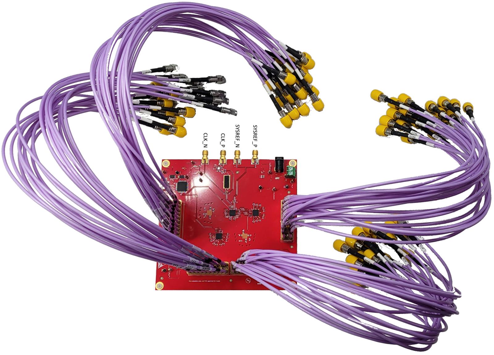
One aspect taken into consideration for this design was the board size, which was heavily determined by the number of inputs and outputs this design requires. As shown in Figure 1-2, the design uses the Samtec Bull's Eye Connector to ease the board size constraint created by 40 output differential pairs. All 20 outputs of a single LMX1204 device pass through a connector that takes up only 630mm2, less than 1/4 of the equivalent PCB footprint using typical edge mounted SMA connectors.
 Figure 1-2 LMX1204 Clock Distribution
Board