SLUAAJ7 June   2022 UCC256402 , UCC256403 , UCC256404


  1.   Abstract
  2.   Trademarks
  3. 1UCC25640x Selection Guide
  4. 2UCC25640x Features Brief Overview
    1. 2.1 High Voltage(HV) Startup
      1. 2.1.1 HV Startup Procedure
      2. 2.1.2 HV Startup with External Bias
      3. 2.1.3 HV Start-up, VCC, X-cap Discharge Internal Block Diagram
      4. 2.1.4 HV Startup External Resistor
    2. 2.2 XCAP Discharge
      1. 2.2.1 IEC Standards
      2. 2.2.2 Detecting AC presence
      3. 2.2.3 Test Current Injection for Zero Crossing Detection
      4. 2.2.4 Typical Waveforms of HV Startup and XCAP Discharge
    3. 2.3 Feedback Chain
      1. 2.3.1 FBreplica Generation
      2. 2.3.2 Vcomp Signal and Threshold Voltages
      3. 2.3.3 FB Pin Voltage Typical Waveform at no Load
    4. 2.4 Hybrid Hysteretic Control and VCR Pin Voltage and Gate Pulse Generation
      1. 2.4.1 Hybrid Hysteretic Control
      2. 2.4.2 VCR Pin Voltage
      3. 2.4.3 VCR Typical Waveform
    5. 2.5 Soft Start
      1. 2.5.1 Soft Start Timing
      2. 2.5.2 Soft Start Initial Voltage Programming
    6. 2.6 Burst Mode
      1. 2.6.1 Burst Patterns
      2. 2.6.2 BMTL/BMTH Ratio Programming
      3. 2.6.3 BMTH Generation
      4. 2.6.4 Interpreting BMTL and BMTH
      5. 2.6.5 Soft On or Off
      6. 2.6.6 Operation when Burst Mode Disabled
      7. 2.6.7 Typical Waveforms
    7. 2.7 Adaptive Dead Time Control
    8. 2.8 Fault Management
      1. 2.8.1 OCP Protection
      2. 2.8.2 OCP Fault Typical Waveforms
      3. 2.8.3 Over Voltage Protection using Bias Winding (BW OVP)
      4. 2.8.4 Restart or Latch
    9. 2.9 ZCS Region Prevention Scheme
      1. 2.9.1 ZCS Effects
      2. 2.9.2 ZCS Detection and Prevention and Disabling
  5. 3UCC25640x Power Up Guidelines and Debugging Notes
    1. 3.1  Power Up Procedure
    2. 3.2  HV Pin
    3. 3.3  VCC Pin
    4. 3.4  BLK Pin
    5. 3.5  FB Pin
    6. 3.6  ISNS Pin
    7. 3.7  VCR Pin
    8. 3.8  BW Pin
    9. 3.9  LL/SS Pin
    10. 3.10 LO Pin
    11. 3.11 RVCC Pin
    12. 3.12 HS, HO, HB Pins
  6. 4References

OCP Protection

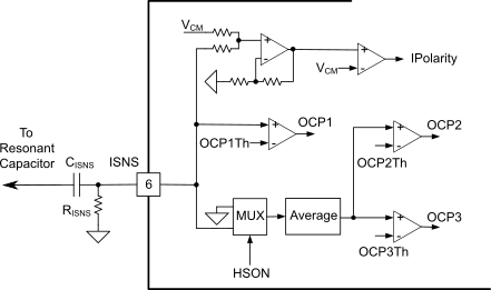
GUID-20220601-SS0I-QMLZ-WBSX-NBSWVXJRS3SF-low.pngFigure 2-33 Over Current Protection (OCP) Protection
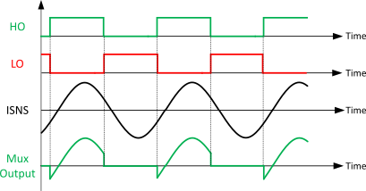
GUID-20220601-SS0I-FBJP-MXGS-BDW4SX2MZ4PL-low.pngFigure 2-34 High Side Switch Current Extraction from ISNS Signal
  • Resonant current is reconstructed as ISNS voltage using a differentiator connected to the resonant capacitor.
  • OCP1 (OCP1Th: 4 V) is for output short circuit protection; it checks the magnitude of the resonant current.
  • OCP2 (OCP2Th: 0.6 V) is for over-load protection; it checks the average DC input current. The time the average input current needs to stay above OCP2 threshold before OCP2 is triggered is 2 ms.
  • OCP3 (OCP3Th: 0.43 V) is also for over-load protection but it has lower threshold value compared to OCP2, OCP1; it checks the average DC input current. The time the average input current needs to stay above OCP3 threshold before OCP3 is triggered is 50 ms.
  • DC input current is reconstructed by capturing the current flowing through high side MOSFET.
  • Internally, ISNS voltage is truncated when HO is high and then filtered to get the average dc value.