SLUAAJ7 June   2022 UCC256402 , UCC256403 , UCC256404


  1.   Abstract
  2.   Trademarks
  3. 1UCC25640x Selection Guide
  4. 2UCC25640x Features Brief Overview
    1. 2.1 High Voltage(HV) Startup
      1. 2.1.1 HV Startup Procedure
      2. 2.1.2 HV Startup with External Bias
      3. 2.1.3 HV Start-up, VCC, X-cap Discharge Internal Block Diagram
      4. 2.1.4 HV Startup External Resistor
    2. 2.2 XCAP Discharge
      1. 2.2.1 IEC Standards
      2. 2.2.2 Detecting AC presence
      3. 2.2.3 Test Current Injection for Zero Crossing Detection
      4. 2.2.4 Typical Waveforms of HV Startup and XCAP Discharge
    3. 2.3 Feedback Chain
      1. 2.3.1 FBreplica Generation
      2. 2.3.2 Vcomp Signal and Threshold Voltages
      3. 2.3.3 FB Pin Voltage Typical Waveform at no Load
    4. 2.4 Hybrid Hysteretic Control and VCR Pin Voltage and Gate Pulse Generation
      1. 2.4.1 Hybrid Hysteretic Control
      2. 2.4.2 VCR Pin Voltage
      3. 2.4.3 VCR Typical Waveform
    5. 2.5 Soft Start
      1. 2.5.1 Soft Start Timing
      2. 2.5.2 Soft Start Initial Voltage Programming
    6. 2.6 Burst Mode
      1. 2.6.1 Burst Patterns
      2. 2.6.2 BMTL/BMTH Ratio Programming
      3. 2.6.3 BMTH Generation
      4. 2.6.4 Interpreting BMTL and BMTH
      5. 2.6.5 Soft On or Off
      6. 2.6.6 Operation when Burst Mode Disabled
      7. 2.6.7 Typical Waveforms
    7. 2.7 Adaptive Dead Time Control
    8. 2.8 Fault Management
      1. 2.8.1 OCP Protection
      2. 2.8.2 OCP Fault Typical Waveforms
      3. 2.8.3 Over Voltage Protection using Bias Winding (BW OVP)
      4. 2.8.4 Restart or Latch
    9. 2.9 ZCS Region Prevention Scheme
      1. 2.9.1 ZCS Effects
      2. 2.9.2 ZCS Detection and Prevention and Disabling
  5. 3UCC25640x Power Up Guidelines and Debugging Notes
    1. 3.1  Power Up Procedure
    2. 3.2  HV Pin
    3. 3.3  VCC Pin
    4. 3.4  BLK Pin
    5. 3.5  FB Pin
    6. 3.6  ISNS Pin
    7. 3.7  VCR Pin
    8. 3.8  BW Pin
    9. 3.9  LL/SS Pin
    10. 3.10 LO Pin
    11. 3.11 RVCC Pin
    12. 3.12 HS, HO, HB Pins
  6. 4References

Test Current Injection for Zero Crossing Detection

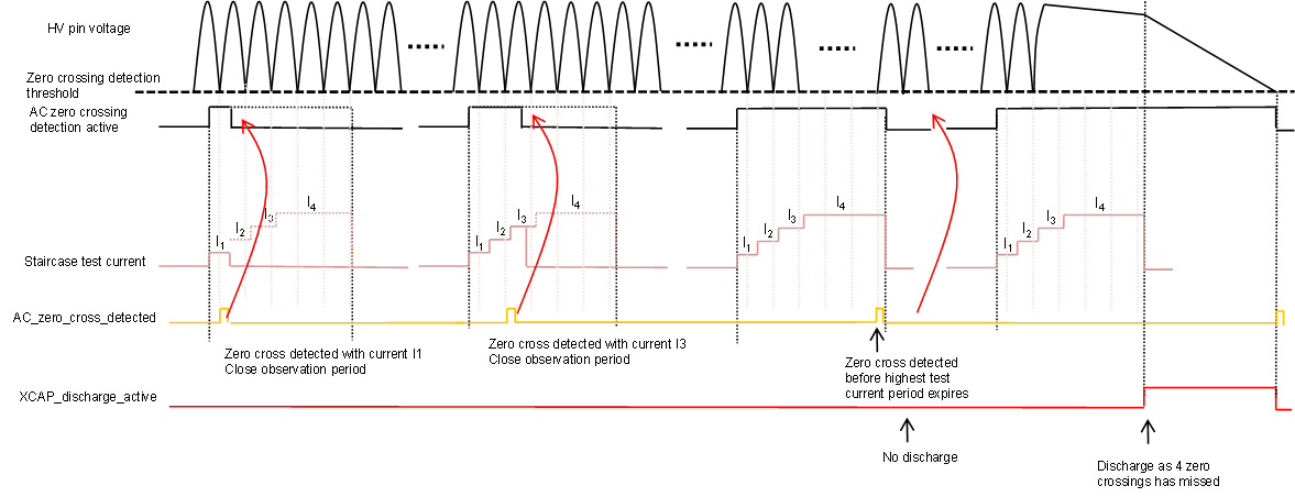
GUID-4E0B17EA-FAD0-4708-AA04-9578641444AF-low.gif Figure 2-7 Xcap Discharge
  • Test current I1 is applied to check if HV pin voltage is <9 V threshold.
  • When HV pin voltage falls below 9 V, test current is turned off and controller waits 700 ms before applying I1 again.
  • I1 test current is on for maximum of 12 ms. If HV pin does not satisfy <9 V requirement, test current is increased to I2, then I3 and finally, I4.
  • I4 test current maximum on time is 48 ms.
  • If zero crossing is not detected during the test current period, a discharge current of 11.5 mA (typical value) is applied for 350 ms from HV to GND as shown in Figure 2-7.