SLUAAF9 September 2021 UCC28782
- Trademarks
- 1 Initial Board Visual Inspection and Start-up Check
- 2 Typical System Operating Waveforms
- 3Typical System Protection Waveforms
- 4Common Issues and Solutions
- 5References
4.3.2 SR MOSFET VDS Overstress at Survival Mode
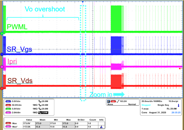
This process could rarely be observed at full load transient to no load, output voltage overshoot results in UCC28782 long time pulse stop, shown in Figure 4-8.VDD drop to around 13-V due to the controller still consume the energy on VDD capacitances even pulse is stopped. While BIN capacitors been over discharged during this time. When survival mode kicks in, most of current flow into BIN pin caps, less current go to SR FET, SR turn on at minimum on time that a reverse current can be seen at it’s turn off edge. This reverse current will trigger next turn on pulse that lead to SR turn on again and again.
 Figure 4-8 SR Vds Overstress When
Survival Mode Kick In
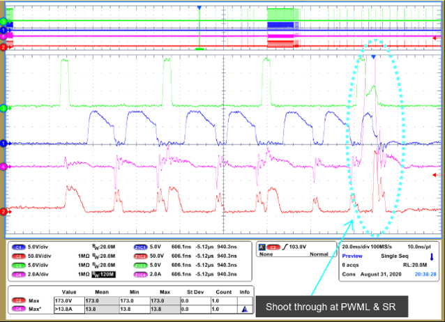
 Figure 4-9 SR Vds Overstress – Zoom
In
Figure 4-9 SR Vds Overstress – Zoom
InWhen PWML turn on at SR minimum on time, the shoot through between primary side low side FET and SR FET happen. SR FET voltage over stress due to sharp di/dt on leakage inductance. See in Figure 4-9
Solution:
- In series a resistor(~2ohm) on AUX rectifier diode path.
- Change the rectifier diode from Schottky to fast recovery diode.
The purpose of two work-arounds is to increase AUX loop impedance to let more current flow into secondary side to prevent SR minimum on time happen. After that, the user have to check at low output voltage no load operation, whether the controller running at survival mode when. Trade-off maybe need to be made between this issue happens and running at survival mode.