SLUAAF9 September   2021 UCC28782


  1.   Trademarks
  2. 1 Initial Board Visual Inspection and Start-up Check
  3. 2 Typical System Operating Waveforms
    1. 2.1 SBP2 Mode
    2. 2.2 SBP1 Mode
    3. 2.3 LPM mode
    4. 2.4 LPM to ABM Mode Transition
    5. 2.5 ABM Mode
    6. 2.6 ABM to AAM Mode Transition
    7. 2.7 AAM Mode
  4. 3Typical System Protection Waveforms
    1. 3.1 Over-Power Protection (OPP)
    2. 3.2 Output Overvoltage Protection (OVP)
    3. 3.3 Output Short-Circuit Protection (SCP)
  5. 4Common Issues and Solutions
    1. 4.1 VDD Boost Converter Survival Mode
      1. 4.1.1 Survival Mode Due To Boost Inductor DCR Too High.
      2. 4.1.2 System Stays In Survival Mode When the Output Voltage is Low Such as 3.3V/5V/9V
    2. 4.2 10% Load Efficiency Might not Meet spec. in USB-PD Application, Especially at 5 V/9 V Output Condition
    3. 4.3 Transient
      1. 4.3.1 BIN/BSW Pin Damage During LPM to ABM Mode Transition
      2. 4.3.2 SR MOSFET VDS Overstress at Survival Mode
      3. 4.3.3 SR MOSFET Vds Voltage Overstress Due to PWMH Partial Turn On At Load Transition
  6. 5References

Over-Power Protection (OPP)

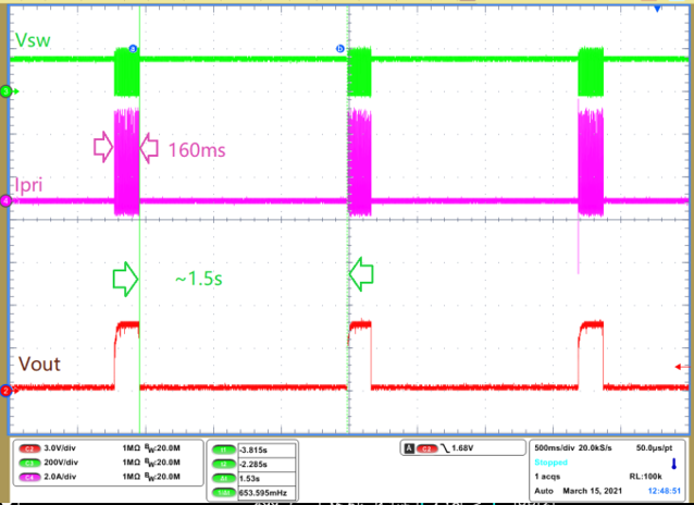
The two key things used to identify what protection happens on the board are delay to action and action, which also listed in UCC28782 data sheet Table 8-3, for OPP, delay to action shown in Figure 3-1is VCST VCST(OPP) and maintain above 160ms, action shown in Figure 3-2is tFDR restart(1.5s).
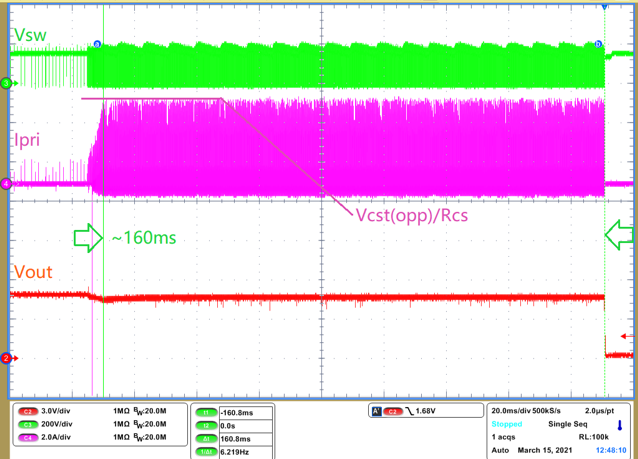
GUID-20210804-CA0I-QZFW-HT46-RC3GRDHLWQKB-low.png Figure 3-1 OPP Delay to Action
GUID-20210804-CA0I-GNJT-XNVN-9TVNZNHRDFQL-low.png Figure 3-2 OPP Action

CH3: Low side FET Vds (Vsw), CH4: Transformer primary winding current (Ipri), CH2: Output voltage (Vout).