SLUAAF9 September   2021 UCC28782


  1.   Trademarks
  2. 1 Initial Board Visual Inspection and Start-up Check
  3. 2 Typical System Operating Waveforms
    1. 2.1 SBP2 Mode
    2. 2.2 SBP1 Mode
    3. 2.3 LPM mode
    4. 2.4 LPM to ABM Mode Transition
    5. 2.5 ABM Mode
    6. 2.6 ABM to AAM Mode Transition
    7. 2.7 AAM Mode
  4. 3Typical System Protection Waveforms
    1. 3.1 Over-Power Protection (OPP)
    2. 3.2 Output Overvoltage Protection (OVP)
    3. 3.3 Output Short-Circuit Protection (SCP)
  5. 4Common Issues and Solutions
    1. 4.1 VDD Boost Converter Survival Mode
      1. 4.1.1 Survival Mode Due To Boost Inductor DCR Too High.
      2. 4.1.2 System Stays In Survival Mode When the Output Voltage is Low Such as 3.3V/5V/9V
    2. 4.2 10% Load Efficiency Might not Meet spec. in USB-PD Application, Especially at 5 V/9 V Output Condition
    3. 4.3 Transient
      1. 4.3.1 BIN/BSW Pin Damage During LPM to ABM Mode Transition
      2. 4.3.2 SR MOSFET VDS Overstress at Survival Mode
      3. 4.3.3 SR MOSFET Vds Voltage Overstress Due to PWMH Partial Turn On At Load Transition
  6. 5References

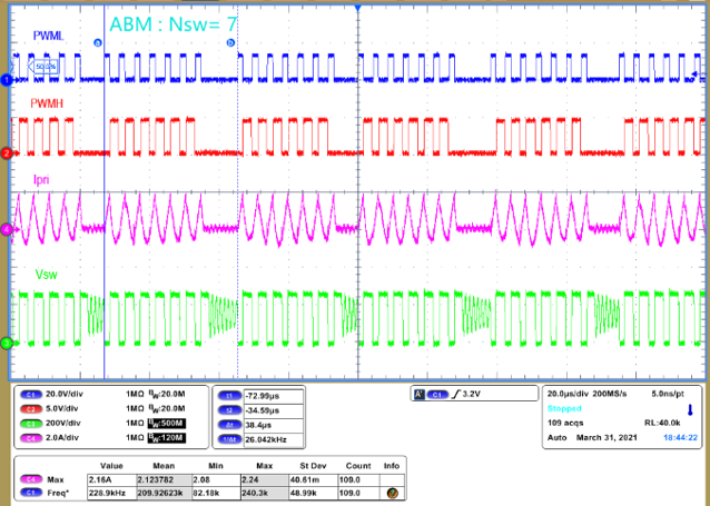
ABM Mode

At ABM mode, the peak current is clamped at VCST(BUR)/Rcs, PWMH is enabled, so Zero-Voltage Switching (ZVS) is achieved except for the first switching cycle. The number of PWML pulses (NSW) is modulated to ensure burst frequency stays above 25khz. As load increases, burst frequency becomes higher and reaches to the high-level burst frequency threshold fBUR(UP), the ABM loop commands NSW to be increased by one pulse to push burst frequency fBUR below fBUR(UP). Additional details can be found in UCC28782 data sheet section 8.4.6.
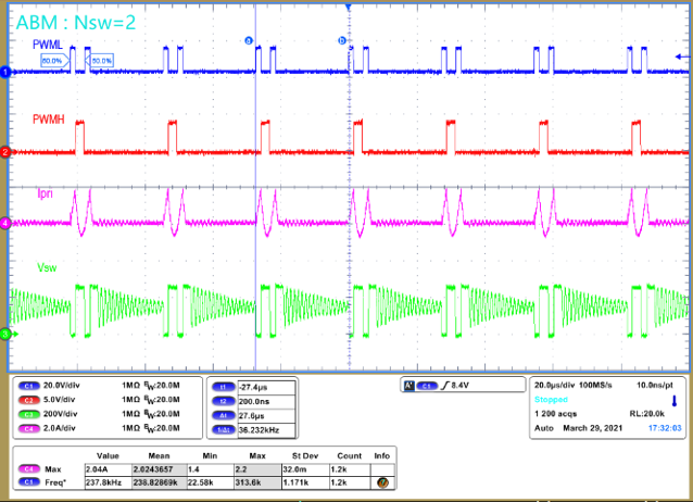
GUID-20210804-CA0I-KBGN-8VQP-HXPPBX2NRN74-low.png Figure 2-5 ABM Mode PWML Pulse NSW=2
GUID-20210804-CA0I-XZDX-PF7S-D1R0FQQDB4XH-low.png Figure 2-6 ABM Mode PWML Pulse NSW=7