SLUAAF9 September 2021 UCC28782
- Trademarks
- 1 Initial Board Visual Inspection and Start-up Check
- 2 Typical System Operating Waveforms
- 3Typical System Protection Waveforms
- 4Common Issues and Solutions
- 5References
4.2 10% Load Efficiency Might not Meet spec. in USB-PD Application, Especially at 5 V/9 V Output Condition
The result could be caused by improper current sense resistor Rcs setting and not using the IPC pin resistor. This process results in a higher burst switching frequency. At 10% load the switching losses become dominant, reduce switching frequency helps reduce switching losses and improve efficiency.
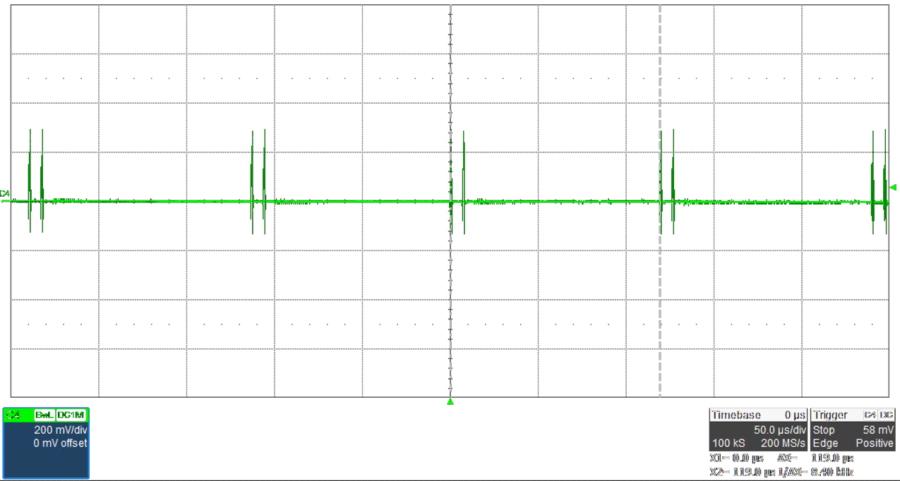
 Figure 4-3 Operating at SBP1 Mode
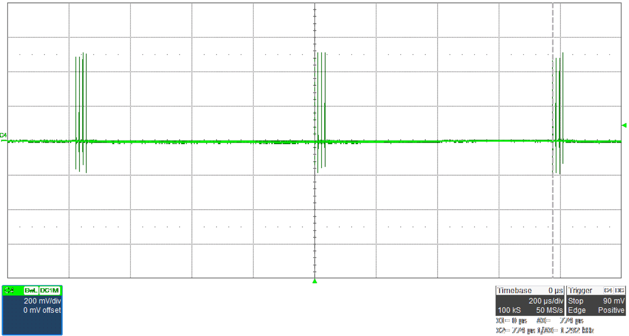
 Figure 4-4 Operating at SBP2 Mode
Solution:
- Reduce current resistor Rcs and increase CS pin filter capacitor Ccs to push
operation mode from SBP1 into SBP2.
Figure 4-3 shows the waveform of SBP1 operation, Figure 4-4 shows the waveform after reducing Rcs or increase Ccs to push Fsw<8 kHz. this helps the system operates at SBP2 mode and improve efficiency significantly.
- Add a resistor between IPC and AGND
Disconnecting a resistor from IPC to AGND is not a mandatory requirement, but connecting a resistor in here helps for improving the light load efficiency especially when 5 V/9 V can’t meet the average efficiency spec.
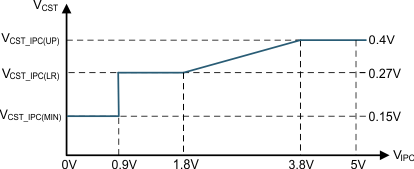
 Figure 4-5 IPC Pin Resistor
Setting
Figure 4-5 IPC Pin Resistor
SettingThere is a 50 uA current source out of the IPC pin, the voltage on IPC pin resistor (VIPC)can program the peak current threshold (VCST_IPC) at SBP2 mode. Higher peak current can further reduce fsw then improve 10% load efficiency, but higher peak current may cause audible noise, trade off between efficiency and noise level maybe need to be made.