SLUAAF9 September   2021 UCC28782


  1.   Trademarks
  2. 1 Initial Board Visual Inspection and Start-up Check
  3. 2 Typical System Operating Waveforms
    1. 2.1 SBP2 Mode
    2. 2.2 SBP1 Mode
    3. 2.3 LPM mode
    4. 2.4 LPM to ABM Mode Transition
    5. 2.5 ABM Mode
    6. 2.6 ABM to AAM Mode Transition
    7. 2.7 AAM Mode
  4. 3Typical System Protection Waveforms
    1. 3.1 Over-Power Protection (OPP)
    2. 3.2 Output Overvoltage Protection (OVP)
    3. 3.3 Output Short-Circuit Protection (SCP)
  5. 4Common Issues and Solutions
    1. 4.1 VDD Boost Converter Survival Mode
      1. 4.1.1 Survival Mode Due To Boost Inductor DCR Too High.
      2. 4.1.2 System Stays In Survival Mode When the Output Voltage is Low Such as 3.3V/5V/9V
    2. 4.2 10% Load Efficiency Might not Meet spec. in USB-PD Application, Especially at 5 V/9 V Output Condition
    3. 4.3 Transient
      1. 4.3.1 BIN/BSW Pin Damage During LPM to ABM Mode Transition
      2. 4.3.2 SR MOSFET VDS Overstress at Survival Mode
      3. 4.3.3 SR MOSFET Vds Voltage Overstress Due to PWMH Partial Turn On At Load Transition
  6. 5References

Output Overvoltage Protection (OVP)

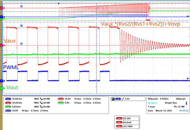
Output voltage is detected by controller through VS pin, However, it is not recommended to probe VS pin directly as the noise introduced by probing could cause protection mis-triggering. Instead, AUX winding voltage can be used for identifying whether OVP happens. If the divided voltage on VS pin exceed OVP threshold for three consecutive pulses, OVP is triggered.
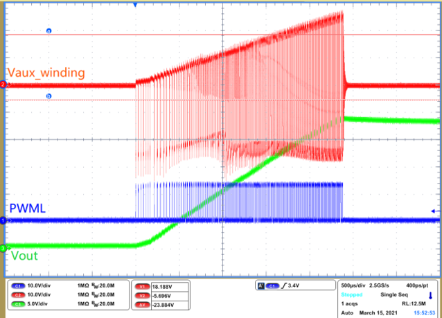
GUID-20210804-CA0I-VB4D-NWGZ-VVXTK9DTBPDP-low.png Figure 3-3 OVP Delay to Action
GUID-20210804-CA0I-FQQN-GHHD-58X2XQFMFK0T-low.png Figure 3-4 OVP Delay to Action (Zoom In)
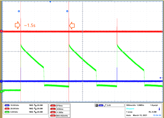
GUID-20210804-CA0I-5K4L-FHZZ-JT2DC5SDTRBR-low.png Figure 3-5 OVP Action

CH2: AUX winding voltage (Vaux), CH1: PWML, CH3: Output voltage.