SLAA602A June 2013 – August 2017 AMC1100 , SM72295 , TMS320F2802-Q1 , TMS320F28027 , TMS320F28027-Q1 , TMS320F28027F , TMS320F28027F-Q1 , TPS54202 , TPS54231
2.2 Switching Waveform Details
To understand the functioning of an Inverter, the user must understand the switching requirement of the four drives of the MOSFETs in H Bridge both in Inverter as well as Mains mode.
1. Inverter Mode
The Switching Wave Form in an Inverter is very simple to understand and generate.
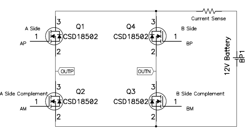 Figure 4. H Bridge Configuration of MOSFETs
 On the A Side MOSFET of the H Bridge, the PWM is generated by modulating the Sine Wave with high frequency (6 KHz to 20 KHz) Square wave in such a way that the positive peak of the Sine Wave is represented by maximum duty cycle and the negative peak by the minimum duty Cycle as shown in Figure 5.
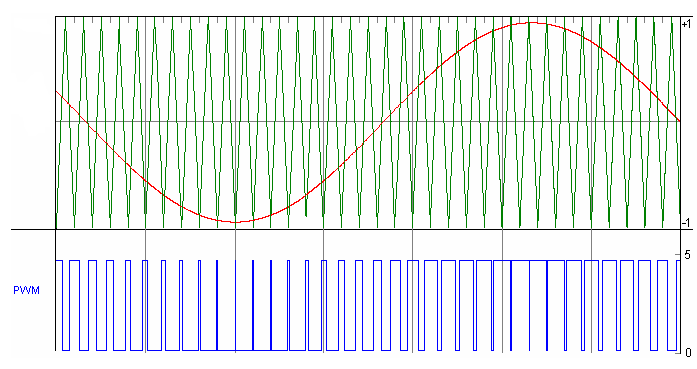 Figure 5. Modulation of Sine Wave With Higher Frequency PWM Signals
 Now on the B Side, just phase shift this Sine Wave by 180 degree and generate the PWM in a similar Way as mentioned above. The following simple hardware implementation of the PWM generation will make the design more clear.
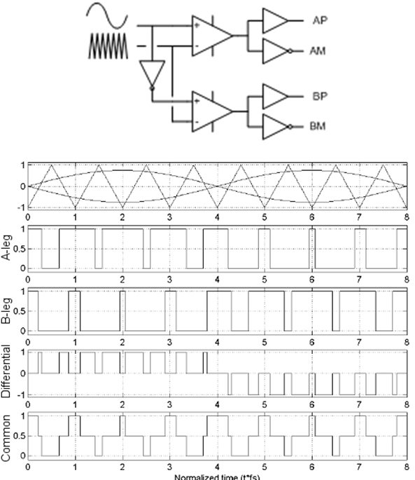 Figure 6. Waveform Generation in Inverter Mode
 A side complementary or the AM signal is obtained by just inverting the A side or AP waveform and the same goes for B Side complementary or BM waveform.
The differential signal seen across the OUTP and OUTN will be a Trilevel PWM Signal as mentioned in Figure 7:
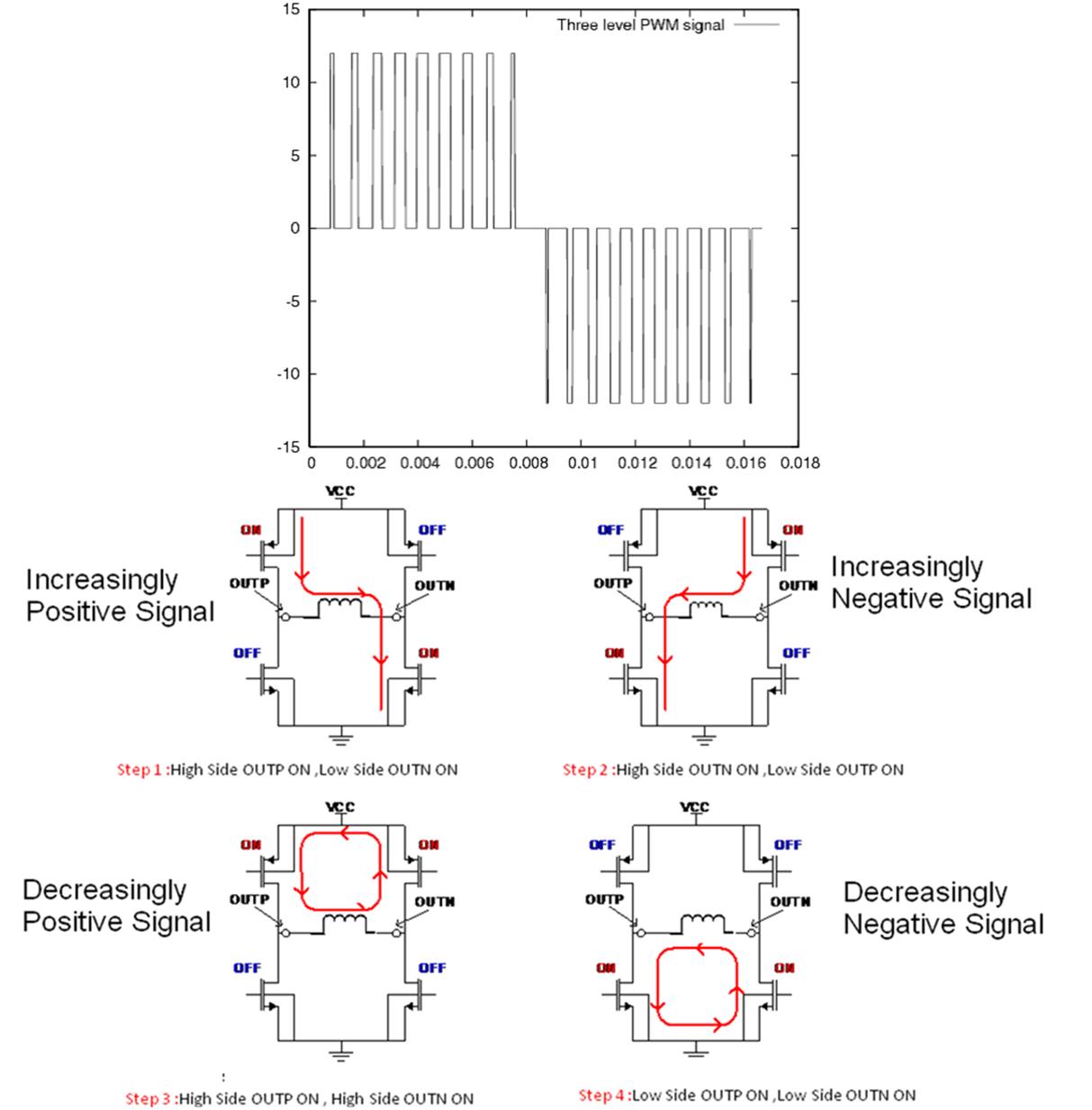 Figure 7. Trilevel PWM Signal During the Inverter Mode for Pure Sine Wave Generation
 2) Mains Mode:
In the mains mode, both the high-side MOSFETs ie A side as well B side is switched off and both the low-side MOSFETs are switched with the similar PWM waveform where the duty cycle of lower side PWM signals determine the charging current.
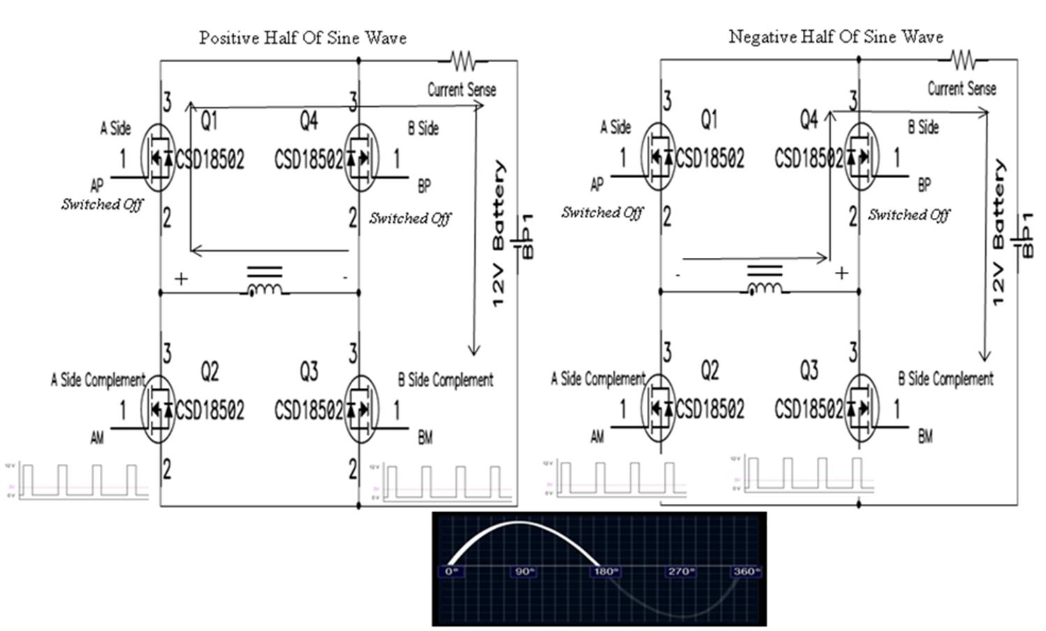 Figure 8. Charging Mode PWM Switching Explanation
 When the lower switches are turned on at the same time, there is a boosted voltage, that appear across the primary leakage inductance of transformer connected to the H–Bridge, by the Ldi/dt effect and this energy is use to charge the battery through the body diodes of the high-side MOSFETs. Also each of the high-side MOSFET’s body diode will conduct in the each half of the Sine Wave.
When the mains mode is sensed, firstly all the MOSFETs are switched off and the Relay between the Ac input and the Inverter output is connected. After this, the Lower FETs are tuned on with PWM of small duty Cycle (5 to 10 percent) and the high-side MOSFETS are switched off. Now the voltage across the current sense is measured by controller and if the corresponding current is less or more than required by charging algorithm than the duty cycle is altered correspondingly ie duty cycle is increased if more charging current is required and decreased if the charging current reduction is desired.