SLAA602A June 2013 – August 2017 AMC1100 , SM72295 , TMS320F2802-Q1 , TMS320F28027 , TMS320F28027-Q1 , TMS320F28027F , TMS320F28027F-Q1 , TPS54202 , TPS54231
2.4 Sections of the Design:
1) 12-V Battery Input to 3.3-V Conversion:
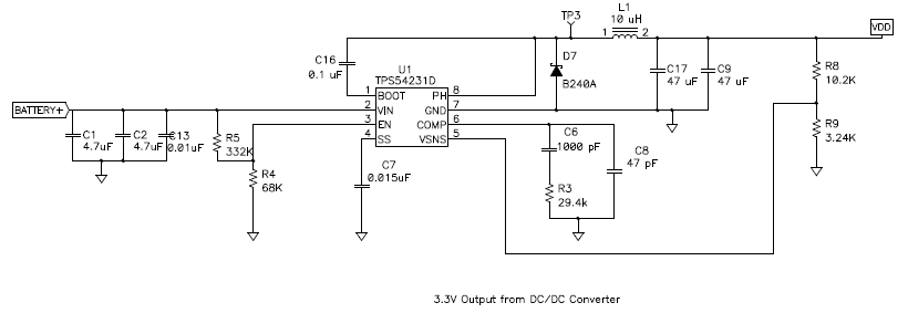
TPS54231 buck converter is used to convert battery voltage (nominal 12 V) to 3.3-V output which in turn is mainly used to power the Controller daughter card and AMC1100 Isolated amplifier secondary side.
The TPS54231 DC-DC converter is designed to provide up to a 2 A (our requirement is a maximum 200 mA) output from an input voltage source of 3.5 V to 28 V, and this integrates a low-RDSon, high-side MOSFET. Further details to the IC can be found from the below links:
TPS54231: 3.5- to 28-V Input, 2-A, 570-kHz Step-Down Converter With Eco-Mode™. Click here to download the data sheet. Below is the design of DC/DC Section:
 Figure 11. DC-DC Converter’s Design
 2) Highly Integrated Gate Driver Design :
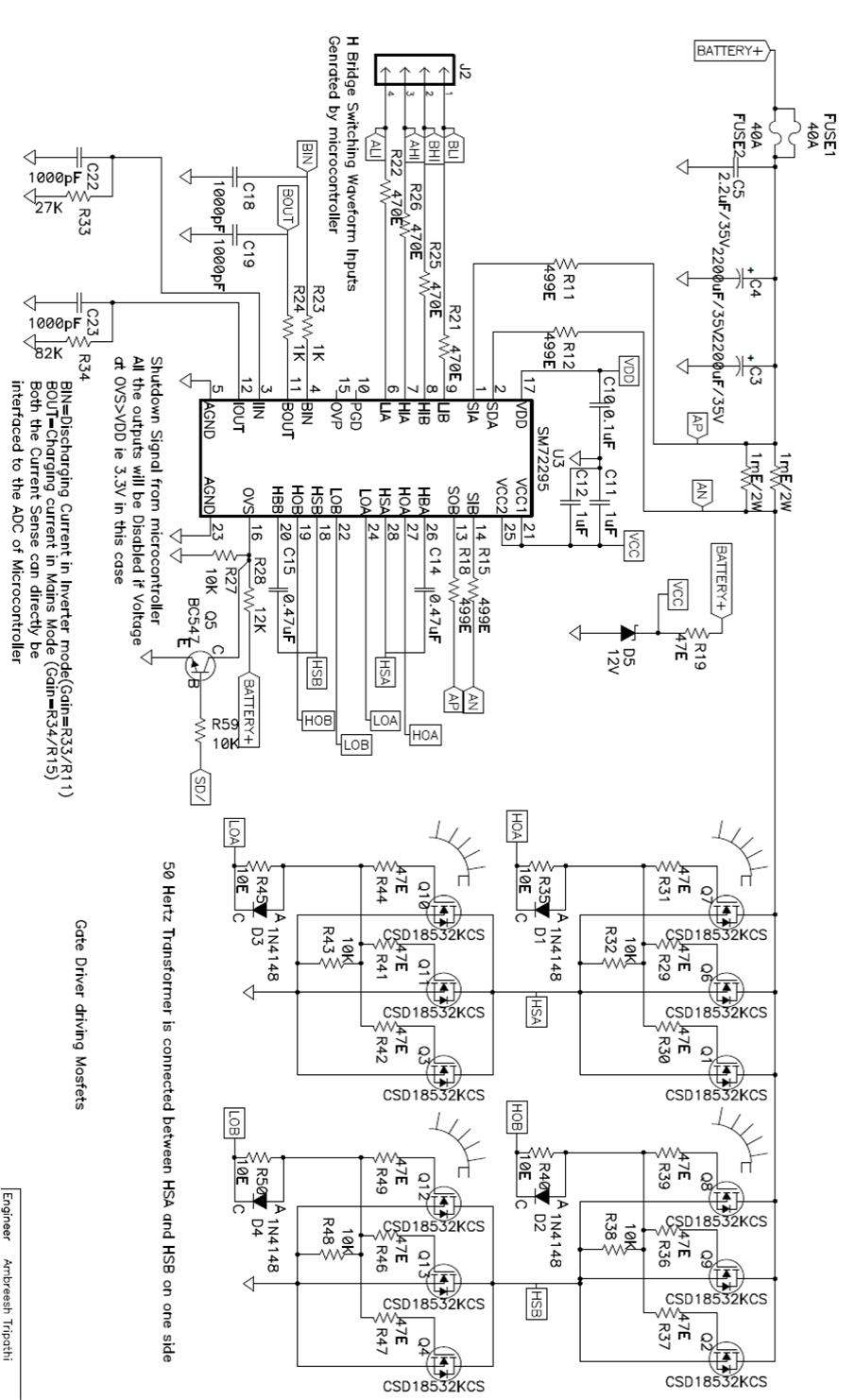
Gate Driver is a power amplifier that accepts a low-power input from a controller IC and produces the appropriate high-current gate drive for a power MOSFET. The gate driver must source and sink current to establish required Vgs.
Here the SM72295 is used as a full bridge MOSFET driver which has 3-A (higher number of FETs in parallel for high power) peak current drive capability and has the following advantages:
1. Integrated ultra-fast, 100-V boot strap diodes (can easily support up to 5KVA rated inverters)
2. Two high side current sense amplifiers with externally programmable gain and buffered outputs which can be used for measuring the battery charge and discharge current – Additional current sense amplifiers and buffers are not required
3. Programmable overvoltage protection – which can be used for charge complete detection or for driver shutdown feature in case of a fault condition
4. Can be directly interfaced with a microcontroller
The complete design principles and circuit details of SM72295 in the Inverter application can be found in the referenced application note (the also includes the current sensing sections of the design):
AN-2296 SM72295: Highly Integrated Gate Driver for 800VA to 3KVA Inverter (SNVA678).
 Figure 12. Gate Driver and Current Sensing
 3) Over Discharge Current and Over Charge Current Protection Implementation:
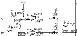
 Figure 13. ODC and OCC Protection
 Here BIN is the voltage across the current sense resistance during the inverter mode and BOUT is the voltage across the current sense during the Mains mode. Now both of these are compared to the different reference voltages, and the PWM is tripped once either BIN or BOUT exceed their given reference voltage.
Setting the reference point during the charging and discharging mode is very simple.
Now with the integrated amplifiers on the SM72295, the gain on the voltage across the current sense during the discharging mode is 27K/499E (ratio of resistance on IIN and SIA pin of SM72295) and during the charging mode is 82K/499E.
To put the over discharge current protection (ODC) at current = 110 A. The drop across the current sense will be current sense resistance × ODC = 0.055 V. Now the gain of 27K/499 is given and the BIN = 3 V approximate. The reference of 3 V is given as ODC protection reference and similarly over charge current protection reference (of 25 A) has been put as 2 V.
4) Input AC Mains Sensing Using Isolated Amplifier:
In the traditional design of Commercial 600 VA - 5 KVA inverters, the AC mains voltage is sensed by stepping down through a bulky 50-Hz transformer by the microcontroller, which is powered up by battery through linear regulators. To ensure the operator safety (personal handling battery, and so on) and signal integrity, galvanic isolation is required in the design.
The input AC Voltage Sensing is required in inverters for changing to Mains mode through relay operation when A/C mains fall in the designated voltage level. Further comparators are also used in addition with transformer for location of zero crossing point of sinusoidal A/C signal.
 Figure 14. AC Mains Sensing Through Isolated Amplifier
 The complete design principles and circuit details of isolated amplifier AMC1100 in the inverter application can be found in the referenced application note:
AMC1100: Replacement of Input Main Sensing Transformer in Inverters with Isolated Amplifier (SLAA552)
5) Relay Operation:
In the mains mode, when the input AC is present and is within valid range, the relay between input AC and the inverter output is closed and the input AC directly goes to the output load. Basically one terminal of the Output (OUTL in this design) is shorted to the line input of the mains and when the relay is turned on neutral get connected to the OUTN and hence the AC input becomes the inverter's output.
 Figure 15. Relay Operation
 6) Inverter’s Output Voltage Sense in Inverter Mode, DC FAN Operation for Cooling MOSFETs and Error Buzzer Operation:
 Figure 16. Output Sense, DC Fan, and Buzzer Operations
 The Output Voltage in Inverter mode is sensed through the Auxiliary winding, which is filtered and rectified and given to the ADC of the microcontroller. When fall in the output voltage is sensed with the increase in the output load, the duty cycle of the H Bridge drive (from microcontroller) is multiplied by a constant greater than 1 so that the final inverter’s output voltage is closer to the no load output voltage (120V/220 VAC) and vice versa on moving from higher load to the lower load.
For example, in this reference design, at no load condition, the duty cycle of the PWM drives given to the H Bridge are varied from 10 percent to 88 percent and when the load is constantly increased at the Inverter’s output, the duty cycle of the PWM is multiplied by a factor greater than 1 so that we can regulate the output voltage within allowable range. While decreasing the load, vice versa followed.
If the duty cycle is increased beyond a point, the output voltage will start clipping, and hence results in higher distortion.Therefore, take care while regulating the output voltage through a feedback.
7) Microcontroller’s Daughter Card:
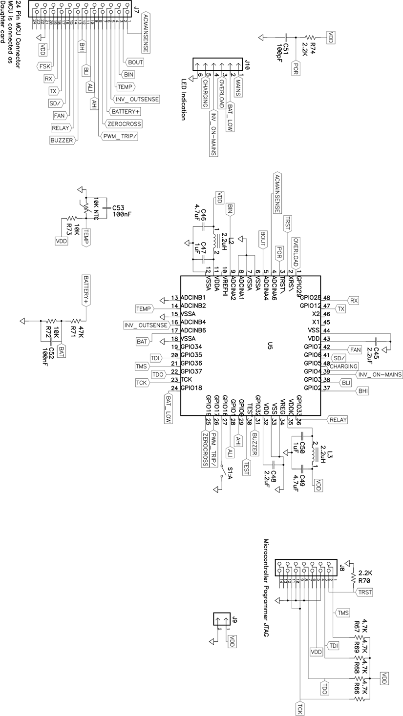
This card has TMS320F280270 MCU, JTAG connector for programming and connector for interfacing all signals with main board. This is a digital power application and most of the MCUs available in the market that finds use in digital power are 16-bit MCUs. TI offers C2000 - 32 bit MCU which can offer good performance which is most wanted in such applications. TMS320F280270PT is C2000 piccolo family MCU series which has unique peripherals like 3 ePWM channels with 6 outputs, 8 channels of the 12-bit, high-speed SAR ADC, 22 digital GPIO shared with digital peripherals with a high performance 50MHz CPU for this application. In this design, all analog and digital pins are being used; however, they can be mapped in different way according to application change if required.
ePWM has Counter compare, action qualifier, dead band, trip zone sub modules with internal connections of channel. Using these central aligned complementary PWM outputs is generated through ePWM output pins with phase shifting of 180 between ePWM1 and ePWM2 channel outputs. TI provides a very efficient IQ match library using which sine wave is generated very easily within fast loop of 50 µS.
This MCU has 12-bit SAR ADC, which can be configured from 7 cycle to 64 cycles long sampling. Using same, one can get very fast feedback signal for adjusting output voltage during inverter mode and charging current in charging mode. ADC is being triggered by 20-KHz PWM, so for every 50 μS, all samples are ready for feedback correction. ADC ISR is being used as control loop function and due to IQ math total time taken for Sine Wave generation, Output correction/charging current correction is around 7 μS.
TMS320F2802x0 I/Os are supported by programmable digital filter for each one of them, making the MCU glitch protected and application development easy with ruggedness.
The Daughter Card is connected to the main board through the 24-pin connector. The controller card performs following main functions:
1. The AC Mains voltage is sensed, and based on this, the relay is operated. (ACMAINSENSE and RELAY)
2. Than the four drives are generated by controller and given to the Gate Driver Inputs. (ALI,BLI,BHI and AHI)
3. The charging current (BOUT) in the mains mode and the discharging current (BIN) in the Inverter mode is continuously tracked and in the error state, PWMs are tripped.
4. Also in the inverter mode, the output voltage of the Inverter is sensed (INV_OUTSENSE) and the duty cycle of the switching PWMs are modified to achieve the regulation in the output voltage.
5. Battery voltage and the temperature of the heat sink is also continuously monitored.
6. Based on the load in the inverter mode or temperature rise of the heat sink, the DC fan is operated.
7. Various LEDs indications are given for user interface.
8. Buzzer is operated if there is any detection of error state in the main board.
 Figure 17. Daughter Card’s Schematic