SLAA602A June 2013 – August 2017 AMC1100 , SM72295 , TMS320F2802-Q1 , TMS320F28027 , TMS320F28027-Q1 , TMS320F28027F , TMS320F28027F-Q1 , TPS54202 , TPS54231
2.5 Required Steps While Debugging/Working on the Hardware
1. The main power board must be checked first, and therefore, the daughter card must not be placed initially. Also, all the initial testing should be done on current limited Lab Power Supply
2. The DC-DC output on the main board is checked for 3.3-V output. Than both (the logic voltage VDD and VCC) the power supply of the SM72295 is checked. The voltage at VCC1 and VCC2 of SM72295 should be 10.5 V with the 12-V input battery.
3. The daughter card should be programmed with the basic inversion software to generate required 4 drives to operate the H – Bridge. Before inserting the Daughter card, the fuse F1 should be removed so that the PWM switching can be seen at the gates of each of the MOSFETs.
4. Now the input drives to the microcontroller be compared with the gates waveform and it is needed to be insured that A side waveform is complementary to the A side complementary waveform and similar for the B side waveform.
5. Now the fuse should be placed on the main board so the H – Bridge gets connected to the power supply. Again all the gates of the MOSFETs has to be monitored. The low-side FETs will be switching at 12-V rail while the high-side FETs will switched at higher rail (gate voltage must be 6 to 12 V higher than the source voltage (12 V), which is achieved through boot strap circuits of the gate driver).
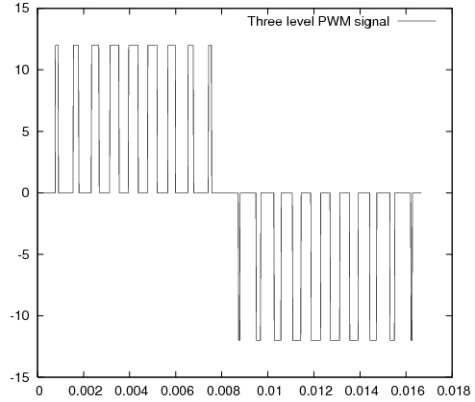
6. The differential signal seen across the high-side MOSFETs sources (OUTP and OUTN) will be a Trilevel PWM signal as mentioned below:
 Figure 18. TITLE??
 7. Now the 50-Hz boost transformer is placed across OUTP and OUTN and the output is filtered through 1-μF/400-VAC capacitors at the inverter output. The inverter output should give 220-V AC signal. Auxillary winding output at INV_OUTSENSE be noted and used to program the feedback loop to have regulated output.
8. The current sense amplification is checked in the inverter mode and the over discharge current protection is tested by increasing load at the output. (Until the no load condition at the output is met??, the lab power supply can be used, and when increasing the load, the 12-V/150-AH battery can be used)
9. All the above stated steps are for the basic inverter testing of the design. The steps below are required for the main mode testing.
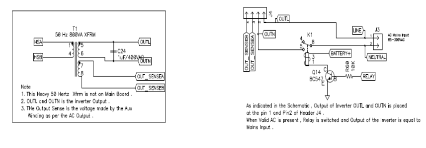
10. Initially, the output of the inverter is not connected to Pin 1 and 2 of Connector J4. The priority is to first check the relay operation. Now when AC input is given to connector J3, it is sensed through the AMC1100, the output of which is connected to the ADC of the microcontroller. Once it is in valid range, firstly all the inverter mode PWM switching is stopped and the relay is switched.
 Figure 19. TITLE?
 11. The output of the Inverter (that is, OUTL and OUTN) is connected to Pin 1 and Pin 2 of the Connector J4, hence why the mains Input becomes the inverter output through the switched relay.
12. After this, the lower FETs are tuned on with a small duty (5 to 10 percent) and the high-side\MOSFETS are switched off. Now the voltage across the current sense is measured by controller and if the corresponding current is less or more required by charging algorithm than the duty cycle is altered correspondingly that is, duty cycle is increased if more charging current is required and decreases if the charging current reduction is desired.
13. Finally, the switching between the Inverter mode and mains mode is checked by inserting or removing the Input AC mains signals.