SLAA602A June 2013 – August 2017 AMC1100 , SM72295 , TMS320F2802-Q1 , TMS320F28027 , TMS320F28027-Q1 , TMS320F28027F , TMS320F28027F-Q1 , TPS54202 , TPS54231
2.1.1 Inverter Mode:
The method, in which the low voltage DC power is inverted, is completed in two steps. The first step is the conversion of the low voltage DC power to a high voltage DC source, and the second step is the conversion of the high DC source to an AC waveform using pulse width modulation. Another method to complete the desired outcome would be to first convert the low voltage DC power to AC, and then use a transformer to boost the voltage to 120/220 volts. The widely used method in the current residential inverter is the second one and hence this reference design is based on this method.
The AC input is sensed through isolated amplifier (AMC1100) and the isolated replica of the AC input is given to the TI’s Picolo Lite Microcontroller ADC. When the AC input is not present in Valid range (Inverter mode) or AC fails, the relay between Mains AC Input and the Inverter Output remain open, the microcontroller generates PWMs and send four drives output to Gate Driver (SM72295). Now the Gate Driver accepts low-power inputs from the controller and produces the appropriate high-current gate drive for the power MOSFETs placed in Full Bridge Topology.
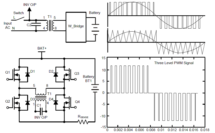
Here H-bridge circuit converts battery DC voltage into AC using high frequency PWM (6 kHz to 20 KHz) thus feeding the 50-Hz transformer which Boost it to 120V/220V AC. The output of transformer contains a capacitor which filters it to make clean 50-Hz AC.
 Figure 3. Inverter Mode Gate Drives
 As seen from the Block Diagram (Figure 3), the Output Voltage is Sensed through the Auxiliary Secondary Winding and feeds to the Controller. The Controller takes this feedback and then Work on the PWM to generate the regulated AC output.
Furthermore the current that is flowing through the battery in Inverter mode and the Charging current during the Mains mode is measured using Integrated Amplifiers of SM72295 and given to the ADCs of the Microcontroller.
Also this reference design has additional protection for Over current Discharge (OCD) and Over Current Charge (OCC) using LM339 Comparators where the amplified Voltage output across Current sense is compared with a pre determined Value and the PWM is immediately shut down by the controller if either the OCD or OCC limit is crossed .