SLAA476B February 2011 – July 2019 BQ2040 , BQ2040 , BQ2060A , BQ2060A , BQ2063 , BQ2063 , BQ2083-V1P3 , BQ2083-V1P3 , BQ2084-V143 , BQ2084-V143 , BQ2084-V150 , BQ2084-V150 , BQ2085-V1P3 , BQ2085-V1P3 , BQ20Z40-R1 , BQ20Z40-R1 , BQ20Z70-V160 , BQ20Z70-V160 , BQ20Z80A-V110 , BQ20Z80A-V110 , BQ28400 , BQ28400 , BQ78PL114 , BQ78PL114 , BQ78PL116 , BQ78PL116 , LM5145 , LM5145 , MSP430F5500 , MSP430F5500 , MSP430F5501 , MSP430F5501 , MSP430F5502 , MSP430F5502 , MSP430F5503 , MSP430F5503 , MSP430F5504 , MSP430F5504 , MSP430F5505 , MSP430F5505 , MSP430F5506 , MSP430F5506 , MSP430F5507 , MSP430F5507 , MSP430F5508 , MSP430F5508 , MSP430F5509 , MSP430F5509 , MSP430F5510 , MSP430F5510 , TPS40057 , TPS40057 , TPS40170 , TPS40170
-
Wide-Vin Battery Charger Using SMBus Communication Interface Between MSP430™ MCUs and bq Fuel Gauges
- Trademarks
- 1 Introduction
- 2 Hardware
- 3
Software
- 3.1 SMBus Protocol Description
- 3.2 Software File Structure
- 3.3
API Calls Description
- 3.3.1 UCS_Init ( )
- 3.3.2 Timer_Init ( )
- 3.3.3 PWM_Init ( )
- 3.3.4 ADC_Init ( )
- 3.3.5 Fan_Init ( )
- 3.3.6 LED_Init ( )
- 3.3.7 SMBus_Initialize ( )
- 3.3.8 LED_Control ( )
- 3.3.9 Fan_Control ( )
- 3.3.10 VI_ADC_Read ( )
- 3.3.11 SMBus_Select ( )
- 3.3.12 Calibrate_Battery ( )
- 3.3.13 Delay_Timer ( )
- 3.3.14 PWM_Control ( )
- 3.3.15 Smbus_Access ( )
- 3.3.16 Smbus_Access_PEC ( )
- 3.3.17 crc8MakeBitwise ( )
- 3.4 Sample Application Description
- 4 SBS Supported Commands Using SMBus Protocol
- 5 Detailed Sample Application Flow Chart
- 6 Battery Status Register Description
- 7 MSP430F5510 Daughterboard Schematics
- 8 Setting Up the MSP430F5510 Daughterboard Hardware
- 9 Battery Calibration Circuit Setup
- 10 Battery Voltage and PWM Conversions
- 11 Battery Current and PWM Conversions
- 12 Power Stage Board Schematics (Generation 1: 40-V Input)
- 13 Bode Plot Measurement for Feedback Loop Stability Analysis
- 14 Power Stage Board Schematics (Generation 2: 60-V Input)
- 15 Setting Up the Power Stage Board Hardware
- 16 References
- Revision History
2.3.3 Constant-Voltage and Constant-Current Feedback
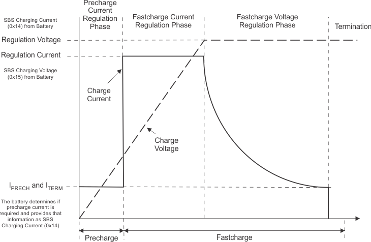
Properly charging a battery requires constant current control followed by constant voltage control as the current tapers. Two separate feedback loops are required to address this requirement (see Figure 6 and Figure 7).
 Figure 6. Typical Charging Profile
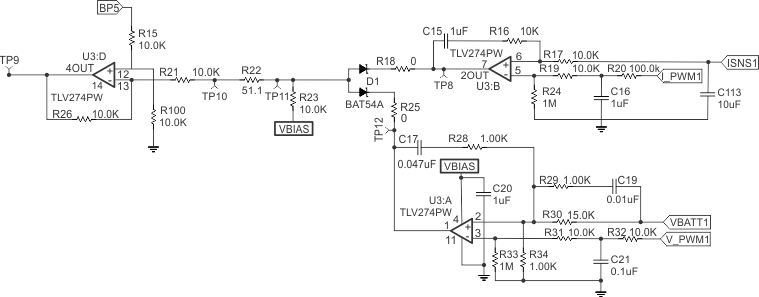
  Figure 7. Constant Current and Voltage Feedback to Charge the Battery
 - The feedback to the TPS40057 is controlled by two loops, one voltage loop and one current loop. Only one of the loops is in control of the power supply at a given time.
- The current and voltage levels are set by the PWM outputs of the MSP430F5510. Duty cycles between 0% and 100% are filtered to produce an analog voltage reference.
- The current into the battery is measured using shunt resistors (R5, R7, and R8) along with an INA193 (U2) (see schematic in Section 12). This circuit provides a voltage that is proportional to the output current (see Equation 1).
- The current sense voltage is then compared to the current reference voltage using U3:B. If the reference voltage is higher, the output of the amplifier is high. If the reference voltage is lower, the output of the amplifier is low.
- The output voltage is measured using a resistor divider (R30 and R34). This voltage is then compared to the output voltage reference. If the reference voltage is higher, the output of the amplifier is high. If the reference voltage is lower, the output of the amplifier is low.
- Diode D1 combines the outputs of the two amplifiers with a logical OR. The voltage that is lowest is fed into an inverting amplifier that makes the error signal polarity correct for the TPS40057 controller.
- The basic operation is that the controller tries to put out a set current, and if the load can accept this current, the controller regulates to that current level. If the load cannot accept the full amount of current, the voltage begins to rise and eventually reaches VOUT_MAX. When this happens, the voltage loop takes over and regulates the output voltage.
For IOUT = 10 A; ISNS = 10 A × 0.025 Ω × 12.1 = 3.33 V
For IOUT = 10 A; ISNS = 10 A × 0.025 Ω × 12.1 = 3.33 V