SLAA475A October 2010 – March 2019 MSP430L092
-
MSP430x09x Analog Pool: Feature Set and Advanced Use
- Trademarks
- 1 MSP430x09x Overview
- 2
Analog Pool (A-Pool)
- 2.1 Input Dividers
- 2.2 Internal Reference
- 2.3 Starting and Stopping the A-Pool
- 2.4 Comparator Function
- 2.5 8-Bit DAC Function
- 2.6 8-Bit ADC Function
- 2.7 SVM Function
- 2.8 Use of Multiple Features
- 2.9 Temperature Measurements With the A-Pool
- 2.10 Fractional and Integer Number Use
- 2.11 APINTB and APFRACTB Use With ATBU and EOCBU
- 2.12 A-Pool Trigger Sources
- 2.13 Filtering ADC Conversions With Digital Filters
- 3 Summary
- 4 References
- Revision History
1 MSP430x09x Overview
The MSP430x09x allows the user to target applications such as motor control, IR communications, and power monitoring. The main differences between the MSP430x09x and other MSP430 MCUs are:
- Native 0.9-V device
- No memory that holds information over a power cycle
- Software ROM module to support loading code to and from external memory
- JTAG pins shared with I/O functionality
- Programmable analog module (A-Pool)
- Emulation mode for ROM code development
- Password protected ROM code
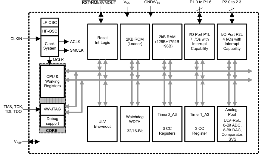
The MSP430x09x consists of several modules (see Figure 1). Two 16-bit timers are available and make it possible to have capture/compare functionality on every port pin. The compact clock system lets you set the correct application frequency. In addition, an analog pool (A-Pool) module is implemented. The A-Pool contains an 8-bit DAC, comparator, and surrounding logic. The A-Pool can be configured to support higher-level functions such as an 8-bit ADC or SVM. Furthermore, 11 I/O pins are available, four of which are used as JTAG communication pins by default. As a software module, the bootloader found in the MSP430L092 allows loading the application code from external memory.
 Figure 1. MSP430L092 Functional Block Diagram