SBAU352 June 2020
6.2 Register Map Configuration Tool
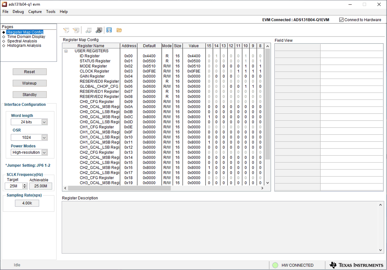
The register map configuration tool allows the user to view and modify the registers of the ADS131B04-Q1. This tool can be selected, as indicated in Figure 13, by clicking on the Register Map Config radio button at the Pages section of the left pane. On power-up, the values on this page correspond to the Host Configuration Settings that enable ADC sampling at the maximum sampling rate specified for the ADC. The register values can be edited by double-clicking the corresponding value field. If interface mode settings are affected by the change in register values, this change reflects on the left pane immediately. The changes in the register value reflect on the AD131M04 device on the ADS131B04-Q1EVM based on the Update Mode selection, as described in Section 6.1.
 Figure 13. Register Map Configuration
 Section 6.3 through Section 6.5 describe the data collection and analysis features of the ADS131B04-Q1EVM GUI.