ZHCS429J March 2012 – November 2021 UCD3138
PRODUCTION DATA
- 1 特性
- 2 应用范围
- 3 说明
- 4 功能方框图
- 5 Revision History
- 6 Device Comparison Table
- 7 Pin Configuration and Functions
- 8 Specifications
-
9 Detailed Description
- 9.1 Overview
- 9.2 ARM Processor
- 9.3 Memory
- 9.4 System Module
- 9.5
Feature Description
- 9.5.1 Sync FET Ramp and IDE Calculation
- 9.5.2 Automatic Mode Switching
- 9.5.3 DPWMC, Edge Generation, IntraMux
- 9.5.4 Filter
- 9.5.5 Communication Ports
- 9.5.6 Miscellaneous Analog
- 9.5.7 Package ID Information
- 9.5.8 Brownout
- 9.5.9 Global I/O
- 9.5.10 Temperature Sensor Control
- 9.5.11 I/O Mux Control
- 9.5.12 Current Sharing Control
- 9.5.13 Temperature Reference
- 9.6 Device Functional Modes
-
10Application and Implementation
- 10.1 Application Information
- 10.2
Typical Application
- 10.2.1 Design Requirements
- 10.2.2 Detailed Design Procedure
- 10.2.3 Application Curves
- 11Power Supply Recommendations
- 12Layout
- 13Device and Documentation Support
- 14Mechanical Packaging and Orderable Information
封装选项
机械数据 (封装 | 引脚)
散热焊盘机械数据 (封装 | 引脚)
订购信息
10.2.2.6.2 Peak Current Detection
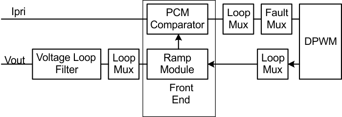
Peak current detection involves all the major modules of the DPPs, the Front End, Filter, Loop Mux, Fault Mux and the DPWMs. A drawing of the major elements is shown in Figure 10-8.
 Figure 10-8 Peak Current Detection Function
All signals without arrows flow from left to right. The voltage loop is used to select a peak current level. This level is fed to the Ramp module to generate a compensation ramp. The compensation ramp is compared to the primary current by the PCMC comparator in the Front End. When the ramp value is greater than the primary current, the APCMC signal is sent to the DPWM, causing the events described in the previous sections.
The DPWM frame start and output pin signals can be used to trigger the Ramp Module. In this case, unlike in the case of other ramp module functions, each DPWM frame triggers the start of the ramp. The ramp steps every 32 ns.
The Filter is configured normally, there is no real difference for PCMC. The PCM_FILTER_SEL bits in the LoopMux.PCMCTRL register are used to select which filter is connected to the ramp module:
LoopMuxRegs.PCMCTRL.bit.PCM_FILTER_SEL =0; //select filter0
With Firmware Constant Power/Constant current, Filter 1 and Front End 1 are used as a current control loop, with the EADCDAC set to high current. If the voltage loop value becomes higher than the current loop value, then Filter 1 is used to control the PCM ramp start value:
LoopMuxRegs.PCMCTRL.bit.PCM_FILTER_SEL =1;
//select filter1 for slope compensation source
In the ramp module, there are 2 bitfields in the RAMPCTRL register which must be configured. The PCM_START_SEL must be set to a 1 to enable the Filter to be used as a ramp start source. The RAMP_EN bit must be set, of course.
The DAC_STEP register sets the slope of the compensation ramp. The DAC value is in volts, of course, so it is necessary to calculate the slope after the current to voltage conversion. Here is the formula for converting from millivolts per microsecond to DACSTEP.
m = compensation slope in millivolts per microsecond
ACSTEP = 335.5 × M
In C, this can be written:
| #define COMPENSATION_SLOPE 150 //compensation slope in millivolts per microsecond #define DACSTEP_COMP_VALUE ((int) (COMPENSATION_SLOPE*335.5) ) //value in DACSTEP for desired compensation slope | |
| FeCtrl0Regs.DACSTEP.all = DACSTEP_COMP_VALUE; | |
It may also be necessary to set a ramp ending value in the RAMPDACEND register.
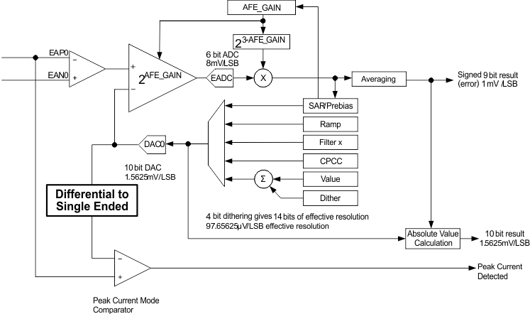
In addition, it is necessary to set the D2S_COMP_EN bit in the EADCCTRL register. This is for enabling the differential to single ended comparator function. The front end diagram leaves it out for simplicity, but the connection between the DAC and the EADC amplifier is actually differential. The PCMC comparator, however, is single ended. So a conversion is necessary as shown in Figure 10-9.
 Figure 10-9 Differential to Single-Ended Comparator Function
The EADC_MODE bit in EADCCTRL should be set to a 5 for peak current mode.
The peak current detection signal next goes to the Loop Mux. The Fault Mux has only 1 APCM input, but there are 3 front ends. So the PCM_FE_SEL bits in APCMCTRL must be used to select which front end is used:
LoopMuxRegs.APCMCTRL.bit.PCM_FE_SEL = 2; // use FE2 for PCM */
The PCM_EN bit must also be set.
LoopMuxRegs.APCMCTRL.bit.PCM_EN = 1; // Enable PCM
Next the Fault Mux is used to enable the APCM bit to the CLIM/CBC signal to the DPWM. There are 4 DPWMxCLIM registers, one for each DPWM. The ANALOG_PCM_EN bit must be set in each one to connect the PCM detection signal to the CLIM/CBC signal on each DPWM. For the latest configuration information on all of these bits, consult the appropriate EVM firmware. To avoid errors, it is best to configure your hardware design using the same DPWMs, filters, and front ends for the same functions as the EVM.
DPWM timing is used to trigger the start of the ramp. This is selected by the FECTRLxMUX registers in the Loop Mux. DPWMx_FRAME_SYNC_EN bits, when set, cause the ramp to be triggered at the start of the DPWM period.