ZHCSMR1C october   2019  – september 2021 UCC5870-Q1

PRODUCTION DATA  

  1. 特性
  2. 应用
  3. 说明
  4. Revision History
  5. Pin Configuration and Functions
  6. Specifications
    1. 6.1  Absolute Maximum Ratings
    2. 6.2  ESD Ratings
    3. 6.3  Recommended Operating Conditions
    4. 6.4  Thermal Information
    5. 6.5  Power Ratings
    6. 6.6  Insulation Specifications
    7. 6.7  Electrical Characteristics
    8. 6.8  SPI Timing Requirements
    9. 6.9  Switching Characteristics
    10. 6.10 Typical Characteristics
  7. Detailed Description
    1. 7.1 Overview
    2. 7.2 Functional Block Diagram
    3. 7.3 Feature Description
      1. 7.3.1 Power Supplies
        1. 7.3.1.1 VCC1
        2. 7.3.1.2 VCC2
        3. 7.3.1.3 VEE2
        4. 7.3.1.4 VREG1
        5. 7.3.1.5 VREG2
        6. 7.3.1.6 VREF
        7. 7.3.1.7 Other Internal Rails
      2. 7.3.2 Driver Stage
      3. 7.3.3 Integrated ADC for Front-End Analog (FEA) Signal Processing
        1. 7.3.3.1 AI* Setup
        2. 7.3.3.2 ADC Setup and Sampling Modes
          1. 7.3.3.2.1 Center Sampling Mode
          2. 7.3.3.2.2 Edge Sampling Mode
          3. 7.3.3.2.3 Hybrid Mode
        3. 7.3.3.3 DOUT Functionality
      4. 7.3.4 Fault and Warning Classification
      5. 7.3.5 Diagnostic Features
        1. 7.3.5.1  Undervoltage Lockout (UVLO) and Overvoltage Lockout (OVLO)
          1. 7.3.5.1.1 Built-In Self Test (BIST)
            1. 7.3.5.1.1.1 Analog Built-In Self Test (ABIST)
            2. 7.3.5.1.1.2 Function BIST
            3. 7.3.5.1.1.3 Clock Monitor
              1. 7.3.5.1.1.3.1 Clock Monitor Built-In Self Test
        2. 7.3.5.2  CLAMP, OUTH, and OUTL Clamping Circuits
        3. 7.3.5.3  Active Miller Clamp
        4. 7.3.5.4  DESAT based Short Circuit Protection (DESAT)
        5. 7.3.5.5  Shunt Resistor based Overcurrent Protection (OCP) and Short Circuit Protection (SCP)
        6. 7.3.5.6  Temperature Monitoring and Protection for the Power Transistors
        7. 7.3.5.7  Active High Voltage Clamping (VCECLP)
        8. 7.3.5.8  Two-Level Turn-Off
        9. 7.3.5.9  Soft Turn-Off (STO)
        10. 7.3.5.10 Thermal Shutdown (TSD) and Temperature Warning (TWN) of Driver IC
        11. 7.3.5.11 Active Short Circuit Support (ASC)
        12. 7.3.5.12 Shoot-Through Protection (STP)
        13. 7.3.5.13 Gate Voltage Monitoring and Status Feedback
        14. 7.3.5.14 VGTH Monitor
        15. 7.3.5.15 Cyclic Redundancy Check (CRC)
          1. 7.3.5.15.1 Calculating CRC
        16. 7.3.5.16 Configuration Data CRC
        17. 7.3.5.17 SPI Transfer Write/Read CRC
          1. 7.3.5.17.1 SDI CRC Check
          2. 7.3.5.17.2 SDO CRC Check
        18. 7.3.5.18 TRIM CRC Check
    4. 7.4 Device Functional Modes
      1. 7.4.1 State 1: RESET
      2. 7.4.2 State 2: Configuration 1
      3. 7.4.3 State 3: Configuration 2
      4. 7.4.4 State 4: Active
    5. 7.5 Programming
      1. 7.5.1 SPI Communication
        1. 7.5.1.1 System Configuration of SPI Communication
          1. 7.5.1.1.1 Independent Slave Configuration
          2. 7.5.1.1.2 Daisy Chain Configuration
          3. 7.5.1.1.3 Address-based Configuration
        2. 7.5.1.2 SPI Data Frame
          1. 7.5.1.2.1 Writing a Register
          2. 7.5.1.2.2 Reading a Register
    6. 7.6 Register Maps
      1. 7.6.1 UCC5870 Registers
  8. Applications and Implementation
    1. 8.1 Application Information
      1. 8.1.1 Power Dissipation Considerations
      2. 8.1.2 Device Addressing
    2. 8.2 Typical Application Using Internal ADC Reference and Power FET Sense Current Monitoring
      1. 8.2.1 Design Requirements
      2. 8.2.2 Detailed Design Procedure
        1. 8.2.2.1 VCC1, VCC2, and VEE2 Bypass Capacitors
        2. 8.2.2.2 VREF, VREG1, and VREG2 Bypass Capacitors
        3. 8.2.2.3 Bootstrap Capacitor (VBST)
        4. 8.2.2.4 VCECLP Input
        5. 8.2.2.5 External CLAMP Output
        6. 8.2.2.6 AI* Inputs
        7. 8.2.2.7 OUTH/ OUTL Outputs
        8. 8.2.2.8 nFLT* Outputs
      3. 8.2.3 Application Curves
    3. 8.3 Typical Application Using DESAT Power FET Monitoring
      1. 8.3.1 Detailed Design Procedure
        1. 8.3.1.1 DESAT Input
      2. 8.3.2 Application Curves
  9. Power Supply Recommendations
    1. 9.1 VCC1 Power Supply
    2. 9.2 VCC2 Power Supply
    3. 9.3 VEE2 Power Supply
    4. 9.4 VREF Supply (Optional)
  10. 10Layout
    1. 10.1 Layout Guidelines
      1. 10.1.1 Component Placement
      2. 10.1.2 Grounding Considerations
      3. 10.1.3 High-Voltage Considerations
      4. 10.1.4 Thermal Considerations
    2. 10.2 Layout Example
  11. 11Device and Documentation Support
    1. 11.1 Documentation Support
      1. 11.1.1 Related Documentation
    2. 11.2 Receiving Notification of Documentation Updates
    3. 11.3 支持资源
    4. 11.4 Trademarks
    5. 11.5 静电放电警告
    6. 11.6 术语表
  12. 12Mechanical, Packaging, and Orderable Information

封装选项

机械数据 (封装 | 引脚)
散热焊盘机械数据 (封装 | 引脚)
订购信息

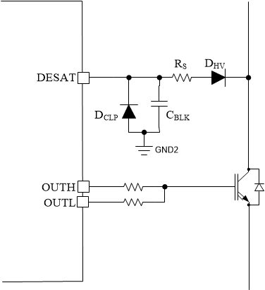
DESAT Input

The DESAT circuit monitors the power module (IGBT for example) for short circuit or over current protection. The external circuit includes four components (Figure 8-8): blanking capacitor (CBLK), clamping diode (DCLP), series resistor RS and high-voltage blocking diode (DHV). CBLK is used to determine the blanking time, tBLK. The time period for tBLK must be long enough to prevent a false trigger when the during the normal operation turn-on cycle. tBLK is calculated as:

Equation 8. tBLK = CBLK × VDESATth/ ICHG

The high voltage diode DHV blocks the high voltage (VCE) while IGBT is OFF. The voltage rating for DHV must be higher than the DC bus voltage plus any switching transient voltage. It is good practice to choose a voltage rating for DHV to be the same or higher than the IGBT voltage rating. Once the proper voltage rating is determined, choose a diode with the least amount of junction capacitance to prevent coupling of DESAT with the dV/dt of the VCE switching. Clamping diode, DCLP, provides a current path to for any coupling current due to the aforementioned junction capacitance of DHV. Select a diode large enough to handle any expected coupling current. The series resistor, RS, dampens any oscillations in the DESAT loop and determines the actual DESAT detection VCE voltage. The actual threshold is calculated as:

Equation 9. VDESAT,ACTUAL = VDESATth - ICHG × RS - VDHV

VDHV is the forward voltage drop of the DHV diode and ICHG is the blanking capacitor charging current selected using the CFG5[DESAT_CHG_CURR] bits.
GUID-F7A397AC-8056-49F5-890B-F7379A0F17C9-low.pngFigure 8-8 External Components for DESAT