ZHCSMR1C october 2019 – september 2021 UCC5870-Q1
PRODUCTION DATA
- 1 特性
- 2 应用
- 3 说明
- 4 Revision History
- 5 Pin Configuration and Functions
- 6 Specifications
-
7 Detailed Description
- 7.1 Overview
- 7.2 Functional Block Diagram
- 7.3
Feature Description
- 7.3.1 Power Supplies
- 7.3.2 Driver Stage
- 7.3.3 Integrated ADC for Front-End Analog (FEA) Signal Processing
- 7.3.4 Fault and Warning Classification
- 7.3.5
Diagnostic Features
- 7.3.5.1 Undervoltage Lockout (UVLO) and Overvoltage Lockout (OVLO)
- 7.3.5.2 CLAMP, OUTH, and OUTL Clamping Circuits
- 7.3.5.3 Active Miller Clamp
- 7.3.5.4 DESAT based Short Circuit Protection (DESAT)
- 7.3.5.5 Shunt Resistor based Overcurrent Protection (OCP) and Short Circuit Protection (SCP)
- 7.3.5.6 Temperature Monitoring and Protection for the Power Transistors
- 7.3.5.7 Active High Voltage Clamping (VCECLP)
- 7.3.5.8 Two-Level Turn-Off
- 7.3.5.9 Soft Turn-Off (STO)
- 7.3.5.10 Thermal Shutdown (TSD) and Temperature Warning (TWN) of Driver IC
- 7.3.5.11 Active Short Circuit Support (ASC)
- 7.3.5.12 Shoot-Through Protection (STP)
- 7.3.5.13 Gate Voltage Monitoring and Status Feedback
- 7.3.5.14 VGTH Monitor
- 7.3.5.15 Cyclic Redundancy Check (CRC)
- 7.3.5.16 Configuration Data CRC
- 7.3.5.17 SPI Transfer Write/Read CRC
- 7.3.5.18 TRIM CRC Check
- 7.4 Device Functional Modes
- 7.5 Programming
- 7.6 Register Maps
- 8 Applications and Implementation
- 9 Power Supply Recommendations
- 10Layout
- 11Device and Documentation Support
- 12Mechanical, Packaging, and Orderable Information
7.3.5.10 Thermal Shutdown (TSD) and Temperature Warning (TWN) of Driver IC
Gate driver temperature monitoring prevents driver IC from damage during overheating conditions. Both the primary and secondary sides of the driver utilize thermal warning and shutdown comparators to help prevent damage due to high temperatures. When a thermal warning is detected on the primary side, the STATUS1[GD_TWN_PRI_FAULT] (STATUS1) is set and, if unmasked, the nFLT2 output is pulled low. If over temperature event is detected on the primary side, the device transitions to the RESET state where the driver output is held low. Once the device cools, the device must be reconfigured as described in the Programming section before enabling the driver output.
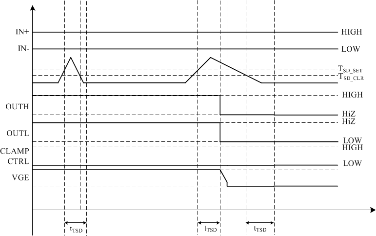
When a thermal warning is detected on the secondary side, the STATUS4[GD_TWN_SEC_FAULT](STATUS4) is set and, if unmasked, the nFLT2 output is pulled low. When a thermal shutdown is detected on the secondary side, the driver is disabled, , the STATUS4[GD_TSD_SEC_FAULT] (STATUS4), is set and, if unmasked, the nFLT1 output is pulled low. The status register flag for TSD may not be set depending on the timing of the thermal event, however the nFLT1 indicator will be pulled low. In the case of the secondary thermal shutdown event, the clock monitor and inter-die communication faults will likely be indicated. This is expected behavior due to the secondary side being shutdown and not communicating to the primary side. Once the driver cools and communication is reestablished, the device must be reconfigured as described in the Programming section before turning on the driver output. A blanking time is inserted to prevent unwanted false triggering of the protection circuits.
 Figure 7-26 Timing scheme of implementation of
driver IC TSD function.