ZHCSMR1C october   2019  – september 2021 UCC5870-Q1

PRODUCTION DATA  

  1. 特性
  2. 应用
  3. 说明
  4. Revision History
  5. Pin Configuration and Functions
  6. Specifications
    1. 6.1  Absolute Maximum Ratings
    2. 6.2  ESD Ratings
    3. 6.3  Recommended Operating Conditions
    4. 6.4  Thermal Information
    5. 6.5  Power Ratings
    6. 6.6  Insulation Specifications
    7. 6.7  Electrical Characteristics
    8. 6.8  SPI Timing Requirements
    9. 6.9  Switching Characteristics
    10. 6.10 Typical Characteristics
  7. Detailed Description
    1. 7.1 Overview
    2. 7.2 Functional Block Diagram
    3. 7.3 Feature Description
      1. 7.3.1 Power Supplies
        1. 7.3.1.1 VCC1
        2. 7.3.1.2 VCC2
        3. 7.3.1.3 VEE2
        4. 7.3.1.4 VREG1
        5. 7.3.1.5 VREG2
        6. 7.3.1.6 VREF
        7. 7.3.1.7 Other Internal Rails
      2. 7.3.2 Driver Stage
      3. 7.3.3 Integrated ADC for Front-End Analog (FEA) Signal Processing
        1. 7.3.3.1 AI* Setup
        2. 7.3.3.2 ADC Setup and Sampling Modes
          1. 7.3.3.2.1 Center Sampling Mode
          2. 7.3.3.2.2 Edge Sampling Mode
          3. 7.3.3.2.3 Hybrid Mode
        3. 7.3.3.3 DOUT Functionality
      4. 7.3.4 Fault and Warning Classification
      5. 7.3.5 Diagnostic Features
        1. 7.3.5.1  Undervoltage Lockout (UVLO) and Overvoltage Lockout (OVLO)
          1. 7.3.5.1.1 Built-In Self Test (BIST)
            1. 7.3.5.1.1.1 Analog Built-In Self Test (ABIST)
            2. 7.3.5.1.1.2 Function BIST
            3. 7.3.5.1.1.3 Clock Monitor
              1. 7.3.5.1.1.3.1 Clock Monitor Built-In Self Test
        2. 7.3.5.2  CLAMP, OUTH, and OUTL Clamping Circuits
        3. 7.3.5.3  Active Miller Clamp
        4. 7.3.5.4  DESAT based Short Circuit Protection (DESAT)
        5. 7.3.5.5  Shunt Resistor based Overcurrent Protection (OCP) and Short Circuit Protection (SCP)
        6. 7.3.5.6  Temperature Monitoring and Protection for the Power Transistors
        7. 7.3.5.7  Active High Voltage Clamping (VCECLP)
        8. 7.3.5.8  Two-Level Turn-Off
        9. 7.3.5.9  Soft Turn-Off (STO)
        10. 7.3.5.10 Thermal Shutdown (TSD) and Temperature Warning (TWN) of Driver IC
        11. 7.3.5.11 Active Short Circuit Support (ASC)
        12. 7.3.5.12 Shoot-Through Protection (STP)
        13. 7.3.5.13 Gate Voltage Monitoring and Status Feedback
        14. 7.3.5.14 VGTH Monitor
        15. 7.3.5.15 Cyclic Redundancy Check (CRC)
          1. 7.3.5.15.1 Calculating CRC
        16. 7.3.5.16 Configuration Data CRC
        17. 7.3.5.17 SPI Transfer Write/Read CRC
          1. 7.3.5.17.1 SDI CRC Check
          2. 7.3.5.17.2 SDO CRC Check
        18. 7.3.5.18 TRIM CRC Check
    4. 7.4 Device Functional Modes
      1. 7.4.1 State 1: RESET
      2. 7.4.2 State 2: Configuration 1
      3. 7.4.3 State 3: Configuration 2
      4. 7.4.4 State 4: Active
    5. 7.5 Programming
      1. 7.5.1 SPI Communication
        1. 7.5.1.1 System Configuration of SPI Communication
          1. 7.5.1.1.1 Independent Slave Configuration
          2. 7.5.1.1.2 Daisy Chain Configuration
          3. 7.5.1.1.3 Address-based Configuration
        2. 7.5.1.2 SPI Data Frame
          1. 7.5.1.2.1 Writing a Register
          2. 7.5.1.2.2 Reading a Register
    6. 7.6 Register Maps
      1. 7.6.1 UCC5870 Registers
  8. Applications and Implementation
    1. 8.1 Application Information
      1. 8.1.1 Power Dissipation Considerations
      2. 8.1.2 Device Addressing
    2. 8.2 Typical Application Using Internal ADC Reference and Power FET Sense Current Monitoring
      1. 8.2.1 Design Requirements
      2. 8.2.2 Detailed Design Procedure
        1. 8.2.2.1 VCC1, VCC2, and VEE2 Bypass Capacitors
        2. 8.2.2.2 VREF, VREG1, and VREG2 Bypass Capacitors
        3. 8.2.2.3 Bootstrap Capacitor (VBST)
        4. 8.2.2.4 VCECLP Input
        5. 8.2.2.5 External CLAMP Output
        6. 8.2.2.6 AI* Inputs
        7. 8.2.2.7 OUTH/ OUTL Outputs
        8. 8.2.2.8 nFLT* Outputs
      3. 8.2.3 Application Curves
    3. 8.3 Typical Application Using DESAT Power FET Monitoring
      1. 8.3.1 Detailed Design Procedure
        1. 8.3.1.1 DESAT Input
      2. 8.3.2 Application Curves
  9. Power Supply Recommendations
    1. 9.1 VCC1 Power Supply
    2. 9.2 VCC2 Power Supply
    3. 9.3 VEE2 Power Supply
    4. 9.4 VREF Supply (Optional)
  10. 10Layout
    1. 10.1 Layout Guidelines
      1. 10.1.1 Component Placement
      2. 10.1.2 Grounding Considerations
      3. 10.1.3 High-Voltage Considerations
      4. 10.1.4 Thermal Considerations
    2. 10.2 Layout Example
  11. 11Device and Documentation Support
    1. 11.1 Documentation Support
      1. 11.1.1 Related Documentation
    2. 11.2 Receiving Notification of Documentation Updates
    3. 11.3 支持资源
    4. 11.4 Trademarks
    5. 11.5 静电放电警告
    6. 11.6 术语表
  12. 12Mechanical, Packaging, and Orderable Information

封装选项

机械数据 (封装 | 引脚)
散热焊盘机械数据 (封装 | 引脚)
订购信息

Device Addressing

When using the Address-based configuration for SPI communication in the system, all devices must be individually addressed. Upon entering the Configuration 1 state (indicated by nFLT* high, assuming no fault during startup), all devices are addressable 0x1 through 0xE (14 unique addresses), with 0xF being a broadcast address to which all devices respond. Addressing is done in the Configuration 1 state. In this state, the IN+ input is pulled high while the WR_CA command is sent with the defined address. The written address is stored in the GDADDRESS[GD_ADDR] bits (GDADDRESS). Once all devices are addressed, send the CFG_IN command with the broadcast device address (0xF) to lock in the device address and move to configuring the devices (Configuration 2 state). The timing diagram for the addressing is shown in Timing diagram for addressing when using the Address-based SPI Communication Scheme..
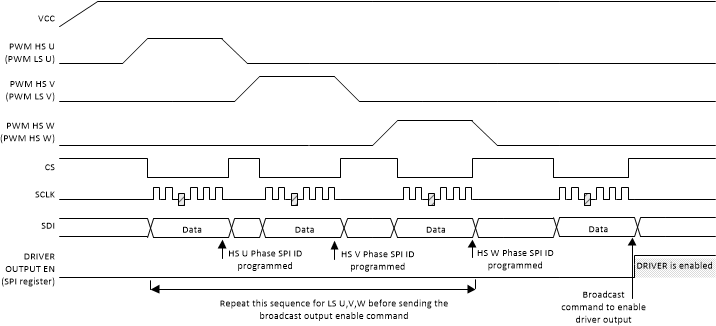
GUID-F5E7CE0A-0779-483E-9CFD-6320FE7562E3-low.pngFigure 8-1 Timing diagram for addressing when using the Address-based SPI Communication Scheme.