ZHCS447C SEPTEMBER 2011 – April 2018 TPS84210
PRODUCTION DATA.
- 1 特性
- 2 应用
- 3 说明
- 4 修订历史记录
- 5 Pin Configuration and Functions
- 6 Specifications
- 7 Functional Block Diagram
- 8 Application and Implementation
- 9 Capacitor Recommendations For The TPS84210 Power Supply
- 10Transient Response
- 11Application Schematics
- 12Power Good (PWRGD)
- 13Power-Up Characteristics
- 14Remote Sense
- 15Output On/Off Inhibit (INH)
- 16Slow Start (SS/TR)
- 17Overcurrent Protection
- 18Synchronization (CLK)
- 19Sequencing (SS/TR)
- 20Programmable Undervoltage Lockout (UVLO)
- 21Thermal Shutdown
- 22Layout Guidelines
- 23Layout Example
- 24EMI
- 25器件和文档支持
- 26机械、封装和可订购信息
5 Pin Configuration and Functions
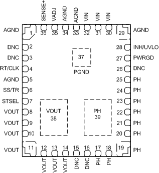
RKG PACKAGE
39 PINS
(TOP VIEW)

Pin Functions
| TERMINAL | DESCRIPTION | |
|---|---|---|
| NAME | NO. | |
| AGND | 1, 5, 29 33, 34 | Zero VDC reference for the analog control circuitry. These pins should be connected directly to the PCB analog ground plane. Not all pins are connected together internally. All pins must be connected together externally with a copper plane or pour directly under the module. Connect the AGND copper area to the PGND copper area at a single point; directly at the pin 37 PowerPAD using multiple vias. See the recommended layout in Figure 34. |
| PowerPAD (PGND) | 37 | This pad provides both an electrical and thermal connection to the PCB. This pad should be connected directly to the PCB power ground plane using multiple vias for good electrical and thermal performance. The same vias should also be used to connect to the PCB analog ground plane. See the recommended layout in Figure 34. |
| DNC | 2, 3, 15, 16, 26 | Do Not Connect. Do not connect these pins to AGND, to another DNC pin, or to any other voltage. These pins are connected to internal circuitry. Each pin must be soldered to an isolated pad. |
| INH/UVLO | 28 | Inhibit and UVLO adjust pin. Use an open drain or open collector output logic to control the INH function. A resistor between this pin and AGND adjusts the UVLO voltage. |
| PH | 17, 18, 19, 20, 21,
22, 23, 24, 25, 39 |
Phase switch node. These pins should be connected by a small copper island under the device for thermal relief. Do not connect any external component to this pin or tie it to a pin of another function. |
| PWRGD | 27 | Power good fault pin. Asserts low if the output voltage is out of tolerance. A pull-up resistor is required. |
| RT/CLK | 4 | This pin automatically selects between RT mode and CLK mode. An external timing resistor adjusts the switching frequency of the device. In CLK mode, the device synchronizes to an external clock. |
| SENSE+ | 36 | Remote sense connection. Connect this pin to VOUT at the load for improved regulation. This pin must be connected to VOUT at the load, or at the module pins. |
| SS/TR | 6 | Slow-start and tracking pin. Connecting an external capacitor to this pin adjusts the output voltage rise time. A voltage applied to this pin allows for tracking and sequencing control. |
| STSEL | 7 | Slow-start or track feature select. Connect this pin to AGND to enable the internal SS capacitor with a SS interval of approximately 1.1 ms. Leave this pin open to enable the TR feature. |
| VADJ | 35 | Connecting a resistor between this pin and AGND sets the output voltage above the 0.8 V default voltage. |
| VIN | 30, 31, 32 | The positive input voltage power pins, which are referenced to PGND. Connect external input capacitance between these pins and the PGND plane, close to the device. |
| VOUT | 8, 9, 10, 11, 12, 13, 14, 38 | Output voltage. Connect output capacitors between these pins and the PGND plane, close to the device. |