ZHCS447C SEPTEMBER 2011 – April 2018 TPS84210
PRODUCTION DATA.
- 1 特性
- 2 应用
- 3 说明
- 4 修订历史记录
- 5 Pin Configuration and Functions
- 6 Specifications
- 7 Functional Block Diagram
- 8 Application and Implementation
- 9 Capacitor Recommendations For The TPS84210 Power Supply
- 10Transient Response
- 11Application Schematics
- 12Power Good (PWRGD)
- 13Power-Up Characteristics
- 14Remote Sense
- 15Output On/Off Inhibit (INH)
- 16Slow Start (SS/TR)
- 17Overcurrent Protection
- 18Synchronization (CLK)
- 19Sequencing (SS/TR)
- 20Programmable Undervoltage Lockout (UVLO)
- 21Thermal Shutdown
- 22Layout Guidelines
- 23Layout Example
- 24EMI
- 25器件和文档支持
- 26机械、封装和可订购信息
18 Synchronization (CLK)
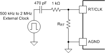
An internal phase locked loop (PLL) has been implemented to allow synchronization between 500 kHz and 2 MHz, and to easily switch from RT mode to CLK mode. To implement the synchronization feature, connect a square wave clock signal to the RT/CLK pin with a minimum pulse width of 75 ns. The maximum clock pulse width must be calculated using Equation 2. The clock signal amplitude must transition lower than 0.4 V and higher than 2.2 V. The start of the switching cycle is synchronized to the falling edge of RT/CLK pin. In applications where both RT mode and CLK mode are needed, the device can be configured as shown in Figure 28.
Before the external clock is present, the device works in RT mode and the switching frequency is set by RT resistor (RRT). When the external clock is present, the CLK mode overrides the RT mode. The device switches from RT mode to CLK mode and the RT/CLK pin becomes high impedance as the PLL starts to lock onto the frequency of the external clock. The device will lock to the external clock frequency approximately 15 µs after a valid clock signal is present. It is not recommended to switch from CLK mode back to RT mode because the internal switching frequency drops to a lower frequency before returning to the switching frequency set by the RT resistor.
|
Equation 2.

|
 Figure 28. CLK/RT Configuration Figure 28. CLK/RT Configuration
|
The synchronization frequency must be selected based on the output voltages of the devices being synchronized. Table 7 shows the allowable frequencies for a given range of output voltages based on a resistive load. 5-V input applications requiring 1.5 A or less can synchronize to a wider frequency range. For the most efficient solution, always synchronize to the lowest allowable frequency. For example, an application requires synchronizing three TPS84210 devices with output voltages of 1.2V@1.7A, 1.8@1.1AV and 3.3V@ 1.0A, all powered from VIN = 5V. Table 7 shows that all three output voltages can be synchronized to any frequency between 700 kHz to 1 MHz. For best efficiency, choose 700 kHz as the sychronization frequency.
Table 7. Synchronization Frequency vs Output Voltage
| SYNCHRONIZATION FREQUENCY (kHz) | RRT (kΩ) | VIN = 5 V | VIN = 3.3 V | ||||
|---|---|---|---|---|---|---|---|
| IOUT ≤ 1.5 A | IOUT> 1.5 A | All IOUT | |||||
| VOUT RANGE (V) | VOUT RANGE (V) | VOUT RANGE (V) | |||||
| MIN | MAX | MIN | MAX | MIN | MAX | ||
| 500 | open | 0.8 | 1.4 | 0.8 | 0.8 | 0.8 | 1.1 |
| 550 | 3400 | 0.8 | 1.6 | 0.8 | 0.9 | 0.8 | 1.2 |
| 600 | 1800 | 0.8 | 1.9 | 0.8 | 1.1 | 0.8 | 2.0 |
| 650 | 1200 | 0.8 | 2.4 | 0.8 | 1.2 | 0.8 | 2.2 |
| 700 | 887 | 0.8 | 3.6 | 0.8 | 1.3 | 0.8 | 2.4 |
| 750 | 715 | 0.9 | 3.6 | 0.9 | 1.5 | 0.8 | 2.5 |
| 800 | 590 | 0.9 | 3.6 | 0.9 | 1.7 | 0.8 | 2.5 |
| 900 | 511 | 1.0 | 3.6 | 1.0 | 2.2 | 0.8 | 2.5 |
| 1000 | 348 | 1.2 | 3.6 | 1.2 | 2.5 | 0.8 | 2.5 |
| 1250 | 232 | 1.4 | 3.6 | 1.4 | 3.3 | 1.0 | 2.5 |
| 1500 | 174 | 1.7 | 3.6 | 1.7 | 3.6 | 1.1 | 2.5 |
| 1750 | 137 | 2.0 | 3.6 | 2.0 | 3.6 | 1.3 | 2.4 |
| 2000 | 113 | 2.3 | 3.6 | 2.3 | 3.6 | 1.5 | 2.3 |