ZHCSKX0 February 2020 TPS59632-Q1
PRODUCTION DATA.
- 1 特性
- 2 应用
- 3 说明
- 4 修订历史记录
- 5 Pin Configuration and Functions
- 6 Specifications
-
7 Detailed Description
- 7.1 Overview
- 7.2 Functional Block Diagram
- 7.3
Feature Description
- 7.3.1 PWM Operation
- 7.3.2 Current Sensing
- 7.3.3 Load-line (Droop)
- 7.3.4 Load Transients
- 7.3.5 Overshoot Reduction (OSR)
- 7.3.6 Undershoot Reduction (USR)
- 7.3.7 Autobalance Current Sharing
- 7.3.8 PWM And SKIP Signals
- 7.3.9 Bias Power (V5A, VDD, And VINTF) UVLO
- 7.3.10 Start-Up Sequence
- 7.3.11 Power Good Operation
- 7.3.12 Analog Current Monitor, IMON, And Corresponding Digital Output Current
- 7.3.13 Fault Behavior
- 7.3.14 Output Under Voltage Protection (UVP)
- 7.3.15 Output Over Voltage Protection (OVP)
- 7.3.16 Over Current Protection (OCP)
- 7.3.17 Over Current Warning
- 7.3.18 Input Voltage Limits
- 7.3.19 VID Table
- 7.4 User Selections
- 7.5 I2C Interface Operation
- 7.6 I2C Register Maps
-
8 Applications and Implementation
- 8.1 Application Information
- 8.2
Typical Application
- 8.2.1
3-Phase D-CAP+™, Step-Down Application
- 8.2.1.1 Design Requirements
- 8.2.1.2
Detailed Design Procedure
- 8.2.1.2.1 Step 1: Select Switching Frequency
- 8.2.1.2.2 Step 2: Set The Slew Rate
- 8.2.1.2.3 Step 3: Set The I2C Address
- 8.2.1.2.4 Step 4: Determine Inductor Value And Choose Inductor
- 8.2.1.2.5 Step 5: Current Sensing Resistance
- 8.2.1.2.6 Step 6: Select Over Current Protection (OCP) Setting
- 8.2.1.2.7 Step 7: Current Monitor (IMON) Setting
- 8.2.1.2.8 Step 8: Set the Load-Line Slope
- 8.2.1.2.9 Step 9: Voltage Feedback Resistor Calculation
- 8.2.1.2.10 Step 10: Ramp Compensation Selection
- 8.2.1.2.11 Step 11 Overshoot Reduction (OSR) selection
- 8.2.1.2.12 Step 12: Undershoot Reduction (USR) selection
- 8.2.1.2.13 Step 13: Loop Compensation
- 8.2.1.3 Application Performance Plots
- 8.2.1
3-Phase D-CAP+™, Step-Down Application
- 9 Power Supply Recommendations
- 10Layout
- 11器件和文档支持
- 12机械、封装和可订购信息
8.2.1.2.9 Step 9: Voltage Feedback Resistor Calculation
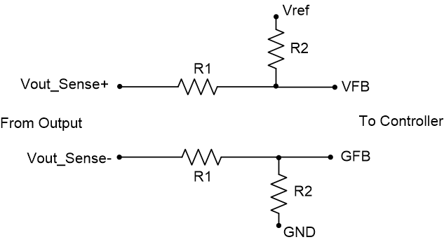
In the device TPS59632-Q1, the internal DAC voltage is set to 0.80 V. To adjust the output voltage above or below this voltage we need to use feedback resistor divider setting. Since we are sensing the voltage using differential remote sense we adopt the circuit shown in Figure 25 to increase the voltage above 0.80 V and the and circuit shown in Figure 26 to decrease the voltage below 0.80 V.
 Figure 25. Feedback resistor divider circuit to increase the output voltage above internal DAC voltage
 In this design, we need to calculate the feedback resistor values, R1 and R2, to increase the voltage above the DAC, the equation shown in Equation 9 is used. Here, VDAC = 0.80 V, and Va from load-line setting is determined as 0.890 V. R2 is set to 10 kΩ and R1 is calculated to 562.

 Figure 26. Feedback resistor divider circuit to decrease the output voltage above internal DAC voltage
 To calculate the feedback resistor values, R1 and R2, to decrease the voltage below the DAC, the equation shown in Equation 10 is used. Here, VDAC = 0.80 V, and Va from load-line setting for the specific application. Vref is the TPS59632-Q1 reference voltage at Pin 27 (VREF) which is nominally 1.7 V. Using this, and setting R2 to 10 kΩ, R1 can be determined.
