ZHCSM34M May   2004  – March 2023 TPS3808

PRODUCTION DATA  

  1. 特性
  2. 应用
  3. 说明
  4. Revision History
  5. Device Voltage Thresholds
  6. Pin Configuration and Functions
  7. Specifications
    1. 7.1 Absolute Maximum Ratings
    2. 7.2 ESD Ratings
    3. 7.3 Recommended Operating Conditions
    4. 7.4 Thermal Information
    5. 7.5 Electrical Characteristics
    6. 7.6 Switching Characteristics
    7. 7.7 Typical Characteristics
  8. Detailed Description
    1. 8.1 Overview
    2. 8.2 Functional Block Diagram
    3. 8.3 Feature Description
      1. 8.3.1 SENSE Input
      2. 8.3.2 Selecting the RESET Delay Time
      3. 8.3.3 Manual RESET ( MR) Input
      4. 8.3.4 RESET Output
    4. 8.4 Device Functional Modes
      1. 8.4.1 Normal Operation (VDD > VDD(min))
      2. 8.4.2 Above Power-On Reset but Less Than VDD(min) (VPOR < VDD < VDD(min))
      3. 8.4.3 Below Power-On Reset (VDD < VPOR)
  9. Application and Implementation
    1. 9.1 Application Information
    2. 9.2 Typical Application
      1. 9.2.1 Design Requirements
      2. 9.2.2 Detailed Design Procedure
        1. 9.2.2.1 Immunity to SENSE Pin Voltage Transients
      3. 9.2.3 Application Curve
  10. 10Power Supply Recommendations
  11. 11Layout
    1. 11.1 Layout Guidelines
    2. 11.2 Layout Example
  12. 12Device and Documentation Support
    1. 12.1 Device Support
      1. 12.1.1 Development Support
        1. 12.1.1.1 Evaluation Modules
    2. 12.2 Documentation Support
      1. 12.2.1 Related Documentation
    3. 12.3 支持资源
    4. 12.4 Trademarks
    5. 12.5 静电放电警告
    6. 12.6 术语表
  13. 13Mechanical, Packaging, and Orderable Information

封装选项

机械数据 (封装 | 引脚)
散热焊盘机械数据 (封装 | 引脚)
订购信息

Typical Characteristics

At TJ = 25°C, VDD = 3.3 V, RLRESET = 100 kΩ, and CLRESET = 50 pF, unless otherwise noted.
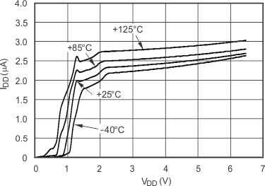
GUID-95D04BDE-A586-4FAB-A764-811C62BD0133-low.gif
Figure 7-2 Supply Current vs Supply Voltage
GUID-80D6632F-A8D6-4457-8B70-D81CA85DCB0C-low.gif
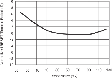
Figure 7-4 Normalized RESET Time-Out Period vs Temperature (CT = Open, CT = VDD, CT = Any)
GUID-AEFC6639-61B9-4CDD-A0BE-A47A05D69B44-low.gif
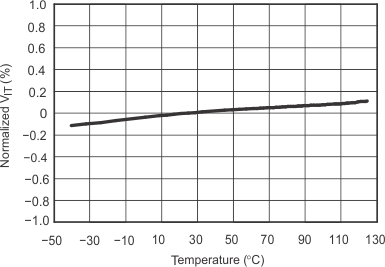
Figure 7-6 Normalized Sense Threshold Voltage (VIT) vs Temperature
GUID-30B9F946-7D35-45DB-A848-54632DA2726E-low.gif
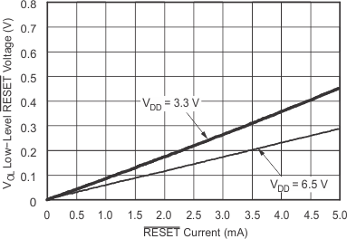
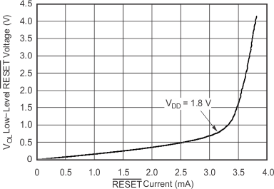
Figure 7-8 Low-Level RESET Voltage vs RESET Current
GUID-D5682ED2-0A59-4563-A6F0-8EA9B145403E-low.gif
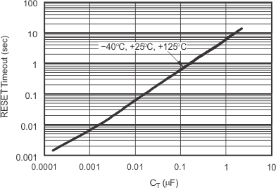
Figure 7-3 RESET Time-Out Period vs CT
GUID-0B82DAE2-79FC-4350-AF44-178933026A74-low.gif
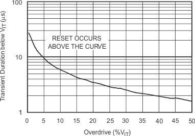
Figure 7-5 Maximum Transient Duration at Sense vs Sense Threshold Overdrive Voltage
GUID-35AF8517-7777-41E0-9ECA-BFA511FA22FE-low.gif
Figure 7-7 Low-Level RESET Voltage vs RESET Current