ZHCSFF5G July 2016 – December 2019 TPS2660
PRODUCTION DATA.
- 1 特性
- 2 应用
- 3 说明
- 4 修订历史记录
- 5 Device Comparison Table
- 6 Pin Configuration and Functions
- 7 Specifications
- 8 Parameter Measurement Information
-
9 Detailed Description
- 9.1 Overview
- 9.2 Functional Block Diagram
- 9.3
Feature Description
- 9.3.1 Undervoltage Lockout (UVLO)
- 9.3.2 Overvoltage Protection (OVP)
- 9.3.3 Reverse Input Supply Protection
- 9.3.4 Hot Plug-In and In-Rush Current Control
- 9.3.5 Overload and Short Circuit Protection
- 9.4 Device Functional Modes
-
10Application and Implementation
- 10.1 Application Information
- 10.2
Typical Application
- 10.2.1 Design Requirements
- 10.2.2 Detailed Design Procedure
- 10.2.3 Application Curves
- 10.3 System Examples
- 10.4 Do's and Don'ts
- 11Power Supply Recommendations
- 12Layout
- 13器件和文档支持
- 14机械、封装和可订购信息
封装选项
请参考 PDF 数据表获取器件具体的封装图。
机械数据 (封装 | 引脚)
- RHF|24
- PWP|16
散热焊盘机械数据 (封装 | 引脚)
订购信息
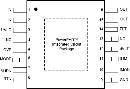
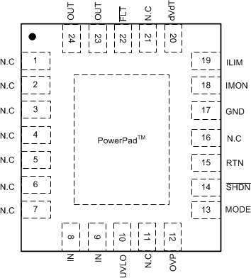
6 Pin Configuration and Functions
PWP Package
16-Pin HTSSOP
Top View

RHF Package
24-Pin VQFN
Top View

Pin Functions
| PIN | TYPE | DESCRIPTION | ||
|---|---|---|---|---|
| NAME | TPS26600/1/2 | |||
| HTSSOP | VQFN | |||
| dVdT | 12 | 20 | I/O | A capacitor from this pin to RTN sets output voltage slew rate See the Hot Plug-In and In-Rush Current Control section |
| FLT | 14 | 22 | O | Fault event indicator. It is an open drain output. If unused, leave floating |
| GND | 9 | 17 | — | Connect GND to system ground |
| ILIM | 11 | 19 | I/O | A resistor from this pin to RTN sets the overload and short-circuit current limit. See the Overload and Short Circuit Protection section |
| IMON | 10 | 18 | O | Analog current monitor output. This pin sources a scaled down ratio of current through the internal FET. A resistor from this pin to RTN converts current to proportional voltage. If unused, leave it floating |
| IN | 1 | 8 | Power | Power input and supply voltage of the device |
| 2 | 9 | |||
| MODE | 6 | 13 | I | Mode selection pin for over load fault response. See the Device Functional Modes section |
| N.C | 4 | 1-7 | — | No connect |
| 13 | 11 | |||
| 16 | ||||
| 21 | ||||
| OUT | 15 | 23 | Power | Power output of the device |
| 16 | 24 | |||
| OVP | 5 | 12 | I | Input for setting the programmable overvoltage protection threshold (For TPS26600/1 only). An overvoltage event turns off the internal FET and asserts FLT to indicate the overvoltage fault. Connect OVP pin to RTN pin externally to select the internal default threshold. For overvoltage clamp response (TPS26602 Only) connect OVP to RTN externally |
| PowerPadTM | — | — | — | PowerPad must be connected to RTN plane on PCB using multiple vias for enhanced thermal performance. Do not use PowerPad as the only electrical connection to RTN |
| RTN | 8 | 15 | — | Reference for device internal control circuits |
| SHDN | 7 | 14 | I | Shutdown pin. Pulling SHDN low makes the device to enter into low power shutdown mode. Cycling SHDN pin voltage resets the device that has latched off due to a fault condition |
| UVLO | 3 | 10 | I | Input for setting the programmable undervoltage lockout threshold. An undervoltage event turns off the internal FET and asserts FLT to indicate the power-failure. Connect UVLO pin to RTN pin to select the internal default threshold |