ZHCSFF5G July 2016 – December 2019 TPS2660
PRODUCTION DATA.
- 1 特性
- 2 应用
- 3 说明
- 4 修订历史记录
- 5 Device Comparison Table
- 6 Pin Configuration and Functions
- 7 Specifications
- 8 Parameter Measurement Information
-
9 Detailed Description
- 9.1 Overview
- 9.2 Functional Block Diagram
- 9.3
Feature Description
- 9.3.1 Undervoltage Lockout (UVLO)
- 9.3.2 Overvoltage Protection (OVP)
- 9.3.3 Reverse Input Supply Protection
- 9.3.4 Hot Plug-In and In-Rush Current Control
- 9.3.5 Overload and Short Circuit Protection
- 9.4 Device Functional Modes
-
10Application and Implementation
- 10.1 Application Information
- 10.2
Typical Application
- 10.2.1 Design Requirements
- 10.2.2 Detailed Design Procedure
- 10.2.3 Application Curves
- 10.3 System Examples
- 10.4 Do's and Don'ts
- 11Power Supply Recommendations
- 12Layout
- 13器件和文档支持
- 14机械、封装和可订购信息
封装选项
请参考 PDF 数据表获取器件具体的封装图。
机械数据 (封装 | 引脚)
- RHF|24
- PWP|16
散热焊盘机械数据 (封装 | 引脚)
订购信息
9.3.1 Undervoltage Lockout (UVLO)
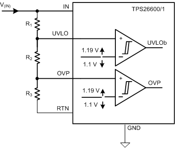
Undervoltage comparator input. When the voltage at UVLO pin falls below V(UVLOF) during input power fail or input undervoltage fault, the internal FET quickly turns off and FLT is asserted. The UVLO comparator has a hysteresis of 90 mV. To set the input UVLO threshold, connect a resistor divider network from IN supply to UVLO terminal to RTN as shown in Figure 34.
 Figure 34. UVLO and OVP Thresholds Set by R1, R2 and R3
 The TPS2660x also features a factory set 15-V input supply undervoltage lockout V(IN_UVLO) threshold with 1 V hysteresis. This feature can be enabled by connecting the UVLO terminal directly to the RTN terminal. If the Under-Voltage Lock-Out function is not needed, the UVLO terminal must be connected to the IN terminal. UVLO terminal must not be left floating.
The device also implements an internal power ON reset (POR) function on the IN terminal. The device disables the internal circuitry when the IN terminal voltage falls below internal POR threshold V(PORF). The internal POR threshold has a hysteresis of 275 mV.