ZHCSA13P November 2008 – February 2021 TMS320F28020 , TMS320F280200 , TMS320F28021 , TMS320F28022 , TMS320F28023 , TMS320F28023-Q1 , TMS320F28026 , TMS320F28026-Q1 , TMS320F28026F , TMS320F28027 , TMS320F28027-Q1 , TMS320F28027F , TMS320F28027F-Q1
PRODUCTION DATA
- 1 特性
- 2 应用
- 3 说明
- 4 功能方框图
- 5 修订历史记录
- 6 Device Comparison
- 7 Terminal Configuration and Functions
- 8 规格
-
9 详细说明
- 9.1
Overview
- 9.1.1 CPU
- 9.1.2 Memory Bus (Harvard Bus Architecture)
- 9.1.3 外设总线
- 9.1.4 Real-Time JTAG and Analysis
- 9.1.5 Flash
- 9.1.6 M0,M1 SARAM
- 9.1.7 L0 SARAM
- 9.1.8 Boot ROM
- 9.1.9 Security
- 9.1.10 外设中断扩展 (PIE) 块
- 9.1.11 外部中断 (XINT1-XINT3)
- 9.1.12 内部零引脚振荡器、振荡器和 PLL
- 9.1.13 看门狗
- 9.1.14 Peripheral Clocking
- 9.1.15 Low-power Modes
- 9.1.16 外设帧 0,1,2 (PFn)
- 9.1.17 通用输入/输出 (GPIO) 复用器
- 9.1.18 32 位 CPU 定时器 (0,1,2)
- 9.1.19 Control Peripherals
- 9.1.20 串行端口外设
- 9.2 Memory Maps
- 9.3 Register Maps
- 9.4 Device Emulation Registers
- 9.5 VREG/BOR/POR
- 9.6 系统控制
- 9.7 Low-power Modes Block
- 9.8 Interrupts
- 9.9
外设
- 9.9.1 Analog Block
- 9.9.2 详细说明
- 9.9.3 Serial Peripheral Interface (SPI) Module
- 9.9.4 Serial Communications Interface (SCI) Module
- 9.9.5 Inter-Integrated Circuit (I2C)
- 9.9.6 Enhanced PWM Modules (ePWM1/2/3/4)
- 9.9.7 High-Resolution PWM (HRPWM)
- 9.9.8 Enhanced Capture Module (eCAP1)
- 9.9.9 JTAG 端口
- 9.9.10 General-Purpose Input/Output (GPIO) MUX
- 9.1
Overview
- 10应用、实施和布局
- 11器件和文档支持
- 12机械、封装和可订购信息
9.9.4 Serial Communications Interface (SCI) Module
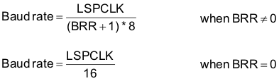
The devices include one serial communications interface (SCI) module (SCI-A). The SCI module supports digital communications between the CPU and other asynchronous peripherals that use the standard nonreturn-to-zero (NRZ) format. The SCI receiver and transmitter are double-buffered, and each has its own separate enable and interrupt bits. Both can be operated independently or simultaneously in the full-duplex mode. To ensure data integrity, the SCI checks received data for break detection, parity, overrun, and framing errors. The bit rate is programmable to over 65000 different speeds through a 16-bit baud-select register.
Features of each SCI module include:
- Two external pins:
- SCITXD: SCI transmit-output pin
- SCIRXD: SCI receive-input pin
Note:
Both pins can be used as GPIO if not used for SCI.
- Baud rate programmable to 64K different rates:
- Data-word format
- One start bit
- Data-word length programmable from 1 to 8 bits
- Optional even/odd/no parity bit
- One or 2 stop bits
- Four error-detection flags: parity, overrun, framing, and break detection
- Two wake-up multiprocessor modes: idle-line and address bit
- Half- or full-duplex operation
- Double-buffered receive and transmit functions
- Transmitter and receiver operations can be accomplished through interrupt-driven or polled algorithms with status flags.
- Transmitter: TXRDY flag (transmitter-buffer register is ready to receive another character) and TX EMPTY flag (transmitter-shift register is empty)
- Receiver: RXRDY flag (receiver-buffer register is ready to receive another character), BRKDT flag (break condition occurred), and RX ERROR flag (monitoring four interrupt conditions)
- Separate enable bits for transmitter and receiver interrupts (except BRKDT)
- NRZ (nonreturn-to-zero) format
Note:
All registers in this module are 8-bit registers that are connected to Peripheral Frame 2. When a register is accessed, the register data is in the lower byte (7–0), and the upper byte (15–8) is read as zeros. Writing to the upper byte has no effect.
Enhanced features:
- Auto baud-detect hardware logic
- 4-level transmit/receive FIFO
The SCI port operation is configured and controlled by the registers listed in Table 9-25.
| NAME(1) | ADDRESS | SIZE (x16) | EALLOW PROTECTED | DESCRIPTION |
|---|---|---|---|---|
| SCICCRA | 0x7050 | 1 | No | SCI-A Communications Control Register |
| SCICTL1A | 0x7051 | 1 | No | SCI-A Control Register 1 |
| SCIHBAUDA | 0x7052 | 1 | No | SCI-A Baud Register, High Bits |
| SCILBAUDA | 0x7053 | 1 | No | SCI-A Baud Register, Low Bits |
| SCICTL2A | 0x7054 | 1 | No | SCI-A Control Register 2 |
| SCIRXSTA | 0x7055 | 1 | No | SCI-A Receive Status Register |
| SCIRXEMUA | 0x7056 | 1 | No | SCI-A Receive Emulation Data Buffer Register |
| SCIRXBUFA | 0x7057 | 1 | No | SCI-A Receive Data Buffer Register |
| SCITXBUFA | 0x7059 | 1 | No | SCI-A Transmit Data Buffer Register |
| SCIFFTXA(2) | 0x705A | 1 | No | SCI-A FIFO Transmit Register |
| SCIFFRXA(2) | 0x705B | 1 | No | SCI-A FIFO Receive Register |
| SCIFFCTA(2) | 0x705C | 1 | No | SCI-A FIFO Control Register |
| SCIPRIA | 0x705F | 1 | No | SCI-A Priority Control Register |
For more information on the SCI, see the Serial Communications Interface (SCI) chapter in the TMS320F2802x,TMS320F2802xx Technical Reference Manual.
Figure 9-33 shows the SCI module block diagram.
 Module Block Diagram") Figure 9-33 Serial Communications Interface (SCI) Module Block Diagram
Figure 9-33 Serial Communications Interface (SCI) Module Block Diagram