ZHCSQV9A August   2022  – April 2024 TMDS1204

PRODUCTION DATA  

  1.   1
  2. 特性
  3. 应用
  4. 说明
  5. Pin Configuration and Functions
  6. Specifications
    1. 5.1 Absolute Maximum Ratings
    2. 5.2 ESD and Latch-Up Ratings
    3. 5.3 Recommended Operating Conditions
    4. 5.4 Thermal Information
    5. 5.5 Electrical Characteristics
    6. 5.6 Timing Requirements
    7. 5.7 Switching Characteristics
    8. 5.8 Typical Characteristics
  7. Parameter Measurement Information
  8. Detailed Description
    1. 7.1 Functional Block Diagram
    2. 7.2 Feature Description
      1. 7.2.1  4-Level Inputs
      2. 7.2.2  I/O Voltage Level Selection
      3. 7.2.3  HPD_OUT
      4. 7.2.4  Lane Control
      5. 7.2.5  Swap
      6. 7.2.6  Linear and Limited Redriver
      7. 7.2.7  Main Link Inputs
      8. 7.2.8  Receiver Equalizer
      9. 7.2.9  CTLE Bypass
      10. 7.2.10 Adaptive Equalization in HDMI 2.1 FRL
        1. 7.2.10.1 HDMI 2.1 TX Compliance Testing with AEQ Enabled
      11. 7.2.11 HDMI 2.1 Link Training Compatible Rx EQ
      12. 7.2.12 Input Signal Detect
        1. 7.2.12.1 SIGDET_OUT Indicator
      13. 7.2.13 Main Link Outputs
        1. 7.2.13.1 Transmitter Bias
        2. 7.2.13.2 Transmitter Impedance Control
        3. 7.2.13.3 TX Slew Rate Control
        4. 7.2.13.4 TX Pre-Emphasis and De-Emphasis Control
        5. 7.2.13.5 TX Swing Control
        6. 7.2.13.6 Fan-out Buffer
      14. 7.2.14 HDMI DDC Capacitance
      15. 7.2.15 DisplayPort
    3. 7.3 Device Functional Modes
      1. 7.3.1 MODE Control
        1. 7.3.1.1 I2C Mode (MODE = "F")
        2. 7.3.1.2 Pin Strap Modes
          1. 7.3.1.2.1 Pin-Strap: HDMI 1.4 and HDMI 2.0 Functional Description
          2. 7.3.1.2.2 Pin-Strap HDMI 2.1 Function (MODE = "0"): Fixed Rx EQ)
          3. 7.3.1.2.3 Pin-Strap HDMI 2.1 Function (Mode = "1"): Flexible Rx EQ
          4. 7.3.1.2.4 Pin-Strap HDMI 2.1 Function (Mode = "R"): Flexible Rx EQ and Fan-Out Buffer
      2. 7.3.2 DDC Snoop Feature
        1. 7.3.2.1 HDMI Type
        2. 7.3.2.2 HDMI 2.1 FRL Snoop
      3. 7.3.3 Low Power States
    4. 7.4 Programming
      1. 7.4.1 Pseudocode Examples
        1. 7.4.1.1 HDMI 2.1 Source Example with DDC Snoop Disabled and DDC Buffer Disabled
        2. 7.4.1.2 Sink Example
      2. 7.4.2 TMDS1204 I2C Address Options
      3. 7.4.3 I2C Target Behavior
    5. 7.5 Register Maps
      1. 7.5.1 TMDS1204 Registers
  9. Application and Implementation
    1. 8.1 Application Information
    2. 8.2 Typical Source-Side Application
      1. 8.2.1 Design Requirements
      2. 8.2.2 Detailed Design Procedure
        1. 8.2.2.1 Pre-Channel (LAB)
        2. 8.2.2.2 Post-Channel (LCD)
        3. 8.2.2.3 Common Mode Choke
        4. 8.2.2.4 ESD Protection
      3. 8.2.3 Application Curves
    3. 8.3 Typical Sink-Side Application
      1. 8.3.1 Design Requirements
      2. 8.3.2 Detailed Design Procedures
    4. 8.4 Power Supply Recommendations
      1. 8.4.1 Supply Decoupling
    5. 8.5 Layout
      1. 8.5.1 Layout Guidelines
      2. 8.5.2 Layout Example
  10. 器件和文档支持
    1. 9.1 文档支持
      1. 9.1.1 相关文档
    2. 9.2 接收文档更新通知
    3. 9.3 支持资源
    4. 9.4 商标
    5. 9.5 静电放电警告
    6. 9.6 术语表
  11. 10Revision History
  12. 11Mechanical, Packaging, and Orderable Information

封装选项

机械数据 (封装 | 引脚)
散热焊盘机械数据 (封装 | 引脚)
订购信息

Application Curves

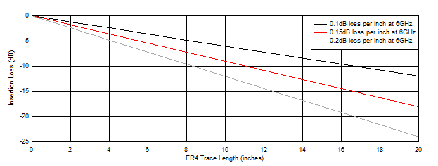
GUID-20200901-CA0I-HG10-NMCL-JH85N0NSNWLM-low.pngFigure 8-3 FR4 Trace Insertion Loss at 6GHz
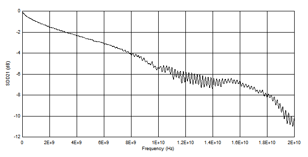
GUID-20220121-SS0I-1LZ3-FLMG-2WHZK5PSJWRB-low.pngFigure 8-5 Post-Channel Insertion Loss at TTP4
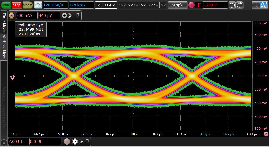
GUID-20220121-SS0I-Q53W-XNKS-C0WKLT05DSPJ-low.pngFigure 8-7 12Gbps Output Eye at TTP4 After Pre and Post Channels
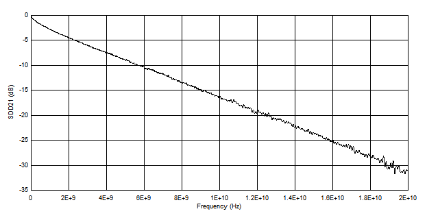
GUID-20220121-SS0I-QTFG-9L8X-SGVBLWVGLVXH-low.pngFigure 8-4 Pre-Channel Insertion Loss at TTP2
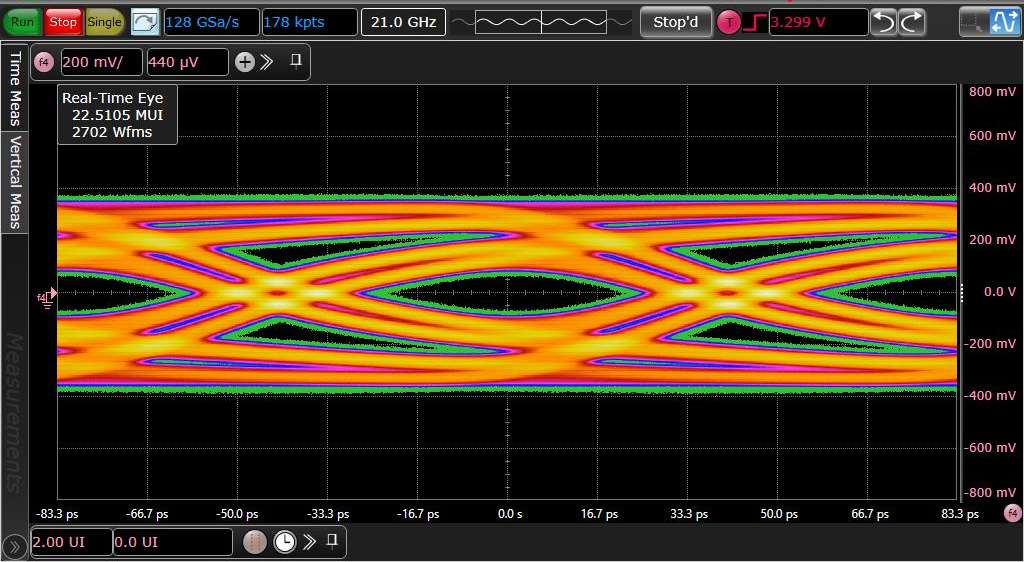
GUID-20220121-SS0I-KVFM-BWQB-LJ30C7N5DCVN-low.pngFigure 8-6 12Gbps Input Eye at TTP2 After Pre-channel
GUID-20220121-SS0I-QR4J-Z38J-LRDX6STJCG2G-low.pngFigure 8-8 12Gbps Output Eye at TTP4_EQ After Pre and Post Channels