ZHCSK83C September 2019 – June 2025 TMCS1100
PRODUCTION DATA
9.2.2 详细设计过程
TMCS1100 应用设计过程有两个关键设计参数:所选的灵敏度版本 (A1-A4) 和基准电压输入。可以进一步考虑噪声和与 ADC 的集成,但这超出了本应用设计示例的范围。TMCS1100 传递函数实际上是一个跨阻,其可变失调电压由 VREF 设置,后者由方程式 28 定义。

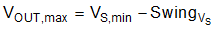
检测器件的设计首先侧重于更大限度地提高器件的灵敏度,同时在预期的电流输入范围内保持线性测量。线性输出电压范围受 TMCS1100 相对于接地的线性摆幅(摆幅GND)和相对于电源的摆幅(摆幅VS)的限制。使用上述参数,最大线性输出电压范围是在 VOUT,max 和 VOUT,min 之间的范围,由方程式 29 和方程式 30 进行定义。

对于双向电流检测应用,从 VREF 至地和电源都需要有足够的线性输出电压范围。表 9-4 展示了该示例应用的设计参数以及计算得出的输出范围。
| 设计参数 | 示例值 |
|---|---|
| 摆幅 VS | 0.2V |
| 摆幅 GND | 0.05V |
| VOUT,max | 4.7V |
| VOUT,min | 0.05V |
| VOUT,max – VOUT,min | 4.65V |
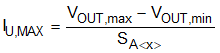
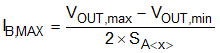
这些设计参数可产生 4.65V 的最大线性输出电压摆幅。若要确定 TMCS1100 的哪个灵敏度型号能够最充分地利用该线性范围,请通过方程式 31 和方程式 32 分别计算单向电流 (IU,MAX) 和双向电流 (IB,MAX) 的最大电流范围。
其中
- SA<x> 为相关 A1-A4 型号的灵敏度。
表 9-5 显示了具有相应灵敏度的 TMCS1100 的每个增益型号的此类计算。
| 灵敏度型号 | 灵敏度 | IU,MAX | IB,MAX |
|---|---|---|---|
| TMCS1100A1 | 50mV/A | 93A | ±46.5A |
| TMCS1100A2 | 100mV/A | 46.5A | ±23.2A |
| TMCS1100A3 | 200mV/A | 23.2A | ±11.6A |
| TMCS1100A4 | 400mV/A | 11.6A | ±5.8A |
通常,选择可提供所需满量程电流范围的最高灵敏度型号。对于本示例中的设计参数,适合选择灵敏度为 0.1V/A 的 TMCS1100A2,因为计算得出的最大线性可测量范围 ±23.2A 足以满足所需的 ±20A 满量程电流要求。
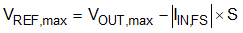
为应用选择合适的灵敏度型号后,可定义由 VREF 输入引脚定义的零电流基准电压。通过操作 方程式 28 和使用由 VOUT,max 和 VOUT,min 定义的线性范围以及满量程输入电流 IIN,FS,计算允许保持在线性测量范围内的最大和最小 VREF 电压,如方程式 33 和方程式 34 所示。
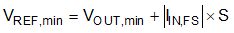
VREF 的任何值都可以在 VREF,max 和 VREF,min 之间选择,从而保持所需的线性检测范围。如果允许的 VREF 范围不够宽或不包括所需的 VREF 电压,则必须使用 TMCS1100 的较低灵敏度型号进行重复分析。通过使用所选的 VREF 电压和最大线性电压范围(如方程式 35 和方程式 36所示)可操作 方程式 28 从而求解任一方向上的最大允许电流。
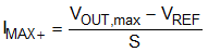
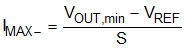
表 9-6 显示了表 9-4 中示例设计参数的相应值。在这种情况下,选择了 2.5V 的 VREF,这样可使零电流输出为标称电源的一半。该示例 VREF 设计值提供 –24.5A 至 +22A 的线性输入电流检测范围,正电流定义为流入 IN+ 引脚的电流。
| 参考参数 | 示例值 | 最大线性电流检测范围 | |
|---|---|---|---|
| IMAX+ | IMAX– | ||
| VREF,min | 2.05V | 26.5A | -20A |
| VREF,max | 2.7V | 20A | -26.5A |
| 所选 VREF | 2.5V | 22A | -24.5A |
为应用设计选择 VREF 后,必须定义适当的源。可有多种实现方式,但可能包括:
- 来自电源电压的电阻分压器
- 来自 ADC 满量程基准的电阻分压器
- 专用或预先存在的电压基准 IC
- 来自系统微控制器的 DAC 或基准电压
每一个选项都有优势,必须权衡每个实现方式的误差项、噪声、简易性和成本。在当前设计示例中,这些选项中的任何一个都可能可用,因为 2.5V VREF 是电源的中轨,这是一种通用 IC 基准电压,并且可能已经在系统中提供。如果当前应用设计的主要考虑事项是最大限度地提高精度,同时最大限度地降低温度漂移和噪声,则必须选择专用电压基准。在这种情况,可以选择 LM4030C-2.5 来优化系统精度,而不会显著增加成本。图 9-3 描述了所介绍的电流检测系统设计。
 图 9-3 TMCS1100 电流检测系统设计示例