ZHCSJB4D April 2019 – January 2024 TAS2563
PRODUCTION DATA
- 1
- 1 特性
- 2 应用
- 3 说明
- 4 Pin Configuration and Functions
-
5 Specifications
- 5.1 Absolute Maximum Ratings
- 5.2 ESD Ratings
- 5.3 Recommended Operating Conditions
- 5.4 Thermal Information
- 5.5 Electrical Characteristics
- 5.6 I2C Timing Requirements
- 5.7 SPI Timing Requirements
- 5.8 PDM Port Timing Requirements
- 5.9 TDM Port Timing Requirements
- 5.10 Timing Diagrams
- 5.11 Typical Characteristics
- 6 Parameter Measurement Information
-
7 Detailed Description
- 7.1 Overview
- 7.2 Functional Block Diagram
- 7.3
Feature Description
- 7.3.1 PurePath Console 3 Software
- 7.3.2 Device Mode and Address Selection
- 7.3.3 General I2C Operation
- 7.3.4 General SPI Operation
- 7.3.5 Single-Byte and Multiple-Byte Transfers
- 7.3.6 Single-Byte Write
- 7.3.7 Multiple-Byte Write and Incremental Multiple-Byte Write
- 7.3.8 Single-Byte Read
- 7.3.9 Multiple-Byte Read
- 7.3.10 Register Organization
- 7.3.11 Operational Modes
- 7.3.12 Faults and Status
- 7.3.13 Digital Input Pull Downs
- 7.4 Device Functional Modes
- 7.5
Register Maps
- 7.5.1 Register Summary Table Page=0x00
- 7.5.2 PAGE (page=0x00 address=0x00) [reset=0h]
- 7.5.3 SW_RESET (page=0x00 address=0x01) [reset=0h]
- 7.5.4 PWR_CTL (page=0x00 address=0x02) [reset=Eh]
- 7.5.5 PB_CFG1 (page=0x00 address=0x03) [reset=20h]
- 7.5.6 MISC_CFG1 (page=0x00 address=0x04) [reset=C6h]
- 7.5.7 MISC_CFG2 (page=0x00 address=0x05) [reset=22h]
- 7.5.8 TDM_CFG0 (page=0x00 address=0x06) [reset=9h]
- 7.5.9 TDM_CFG1 (page=0x00 address=0x07) [reset=2h]
- 7.5.10 TDM_CFG2 (page=0x00 address=0x08) [reset=4Ah]
- 7.5.11 TDM_CFG3 (page=0x00 address=0x09) [reset=10h]
- 7.5.12 TDM_CFG4 (page=0x00 address=0x0A) [reset=13h]
- 7.5.13 TDM_CFG5 (page=0x00 address=0x0B) [reset=2h]
- 7.5.14 TDM_CFG6 (page=0x00 address=0x0C) [reset=0h]
- 7.5.15 TDM_CFG7 (page=0x00 address=0x0D) [reset=4h]
- 7.5.16 TDM_CFG8 (page=0x00 address=0x0E) [reset=5h]
- 7.5.17 TDM_CFG9 (page=0x00 address=0x0F) [reset=6h]
- 7.5.18 TDM_CFG10 (page=0x00 address=0x10) [reset=7h]
- 7.5.19 DSP Mode & TDM_DET (page=0x00 address=0x11) [reset=7Fh]
- 7.5.20 LIM_CFG0 (page=0x00 address=0x12) [reset=12h]
- 7.5.21 LIM_CFG1 (page=0x00 address=0x13) [reset=76h]
- 7.5.22 DSP FREQUENCY & BOP_CFG0 (page=0x00 address=0x14) [reset=1h]
- 7.5.23 BOP_CFG0 (page=0x00 address=0x15) [reset=2Eh]
- 7.5.24 BIL_and_ICLA_CFG0 (page=0x00 address=0x16) [reset=60h]
- 7.5.25 BIL_ICLA_CFG1 (page=0x00 address=0x17) [reset=0h]
- 7.5.26 GAIN_ICLA_CFG0 (page=0x00 address=0x18) [reset=0h]
- 7.5.27 ICLA_CFG1 (page=0x00 address=0x19) [reset=0h]
- 7.5.28 INT_MASK0 (page=0x00 address=0x1A) [reset=FCh]
- 7.5.29 INT_MASK1 (page=0x00 address=0x1B) [reset=A6h]
- 7.5.30 INT_MASK2 (page=0x00 address=0x1C) [reset=DFh]
- 7.5.31 INT_MASK3 (page=0x00 address=0x1D) [reset=FFh]
- 7.5.32 INT_LIVE0 (page=0x00 address=0x1F) [reset=0h]
- 7.5.33 INT_LIVE1 (page=0x00 address=0x20) [reset=0h]
- 7.5.34 INT_LIVE3 (page=0x00 address=0x21) [reset=0h]
- 7.5.35 INT_LIVE4 (page=0x00 address=0x22) [reset=0h]
- 7.5.36 INT_LTCH0 (page=0x00 address=0x24) [reset=0h]
- 7.5.37 INT_LTCH1 (page=0x00 address=0x25) [reset=0h]
- 7.5.38 INT_LTCH3 (page=0x00 address=0x26) [reset=0h]
- 7.5.39 INT_LTCH4 (page=0x00 address=0x27) [reset=0h]
- 7.5.40 VBAT_MSB (page=0x00 address=0x2A) [reset=0h]
- 7.5.41 VBAT_LSB (page=0x00 address=0x2B) [reset=0h]
- 7.5.42 TEMP (page=0x00 address=0x2C) [reset=0h]
- 7.5.43 INT & CLK CFG (page=0x00 address=0x30) [reset=19h]
- 7.5.44 DIN_PD (page=0x00 address=0x31) [reset=40h]
- 7.5.45 MISC (page=0x00 address=0x32) [reset=80h]
- 7.5.46 BOOST_CFG1 (page=0x00 address=0x33) [reset=34h]
- 7.5.47 BOOST_CFG2 (page=0x00 address=0x34) [reset=4Bh]
- 7.5.48 BOOST_CFG3 (page=0x00 address=0x35) [reset=74h]
- 7.5.49 MISC (page=0x00 address=0x3B) [reset=58h]
- 7.5.50 TG_CFG0 (page=0x00 address=0x3F) [reset=0h]
- 7.5.51 BST_ILIM_CFG0 (page=0x00 address=0x40) [reset=36h]
- 7.5.52 PDM_CONFIG0 (page=0x00 address=0x41) [reset=1h]
- 7.5.53 DIN_PD & PDM_CONFIG3 (page=0x00 address=0x42) [reset=F8h]
- 7.5.54 ASI2_CONFIG0 (page=0x00 address=0x43) [reset=8h]
- 7.5.55 ASI2_CONFIG1 (page=0x00 address=0x44) [reset=0h]
- 7.5.56 ASI2_CONFIG2 (page=0x00 address=0x45) [reset=1h]
- 7.5.57 ASI2_CONFIG3 (page=0x00 address=0x46) [reset=FCh]
- 7.5.58 PVDD_MSB_DSP (page=0x00 address=0x49) [reset=0h]
- 7.5.59 PVDD_LSB_DSP (page=0x00 address=0x4A) [reset=0h]
- 7.5.60 REV_ID (page=0x00 address=0x7D) [reset=0h]
- 7.5.61 I2C_CKSUM (page=0x00 address=0x7E) [reset=0h]
- 7.5.62 BOOK (page=0x00 address=0x7F) [reset=0h]
- 8 Application and Implementation
- 9 Power Supply Recommendations
- 10Layout
- 11Device and Documentation Support
- 12Revision History
- 13Mechanical, Packaging, and Orderable Information
封装选项
请参考 PDF 数据表获取器件具体的封装图。
机械数据 (封装 | 引脚)
- YBG|42
- RPP|32
散热焊盘机械数据 (封装 | 引脚)
订购信息
7.4.1 PDM Input
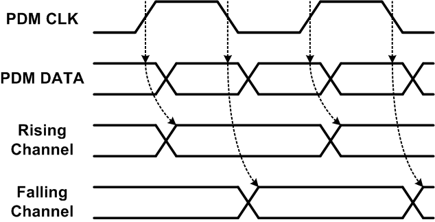
The TAS2563 provides one PDM input. Figure 7-11 below illustrates the double data rate nature of the PDM input. It has two interleaved PDM channels, one sampled by the rising edge and the other by the falling edge of the clock.
 Figure 7-11 PDM Waveform
The PDM inputs are sampled by the PDMCLK pin, which can be configured as either a PDM clock slave input or a PDM clock master output. The PDM_MIC_EDGE and PDM_MIC_SLV register bits select the sample clock edge and master/slave mode PDM inputs. In master mode the PDMCLK pin can disable the clocks (and drive a logic 0) by setting the PDM_GATE_PAD0 register bits low.
When configured as a clock slave, the PDM clock input does not require a specific phase relationship to the system clock (SBCLK in TDM/I2S Mode), but must be from the same source as audio sample rate. This is equivalent to 64/32/16 (~3 MHz) or 128/64/32 (~6 MHz) times a single/double/quadruple speed sample rate. The PDM rate is set by the PDM_RATE_PAD0 .
When PDMCLK pin is configured as a clock master, the TAS2563 will output a 50% duty cycle clock of frequency that is set by the PDM_RATE_PAD0 and register bit (64/32/16 or 128/64/32 times a single/double/quadruple speed sample rate).
| PDM INPUT PIN | REGISTER BIT | VALUE | MASTER/SLAVE |
|---|---|---|---|
| PDMD | PDM_MIC_SLV | | Master |
| Slave (default) |
| PDM CLOCK PIN | REGISTER BIT | VALUE | GATING |
|---|---|---|---|
| PDMCLK | PDM_GATE_PAD0 | | Gated Off (default) |
| Active |
| PDM INPUT PIN | REGISTER BITS | VALUE | SAMPLE RATE |
|---|---|---|---|
| PDMD | PDM_RATE_PAD0 | 0 | 3.072 MHz (default) |
| 6.144 MHz |
| PDM_MIC_EN | MAPPING |
|---|---|
| Disable MIC2 |
| Enable MIC2 |
| Disable MIC1 |
| Enable MIC1 |