ZHCSMY2 December 2020 PCM6480-Q1
PRODUCTION DATA
- 1 特性
- 2 应用
- 3 说明
- 4 Revision History
- 5 Device Comparison Table
- 6 Pin Configuration and Functions
-
7 Specifications
- 7.1 Absolute Maximum Ratings
- 7.2 ESD Ratings
- 7.3 Recommended Operating Conditions
- 7.4 Thermal Information
- 7.5 Electrical Characteristics
- 7.6 Timing Requirements: I2C Interface
- 7.7 Switching Characteristics: I2C Interface
- 7.8 Timing Requirements: SPI Interface
- 7.9 Switching Characteristics: SPI Interface
- 7.10 Timing Requirements: TDM, I2S or LJ Interface
- 7.11 Switching Characteristics: TDM, I2S or LJ Interface
- 7.12 Timing Requirements: PDM Digital Microphone Interface
- 7.13 Switching Characteristics: PDM Digial Microphone Interface
- 7.14 Timing Diagrams
- 7.15 Typical Characteristics
-
8 Detailed Description
- 8.1 Overview
- 8.2 Functional Block Diagram
- 8.3
Feature Description
- 8.3.1 Serial Interfaces
- 8.3.2 Phase-Locked Loop (PLL) and Clock Generation
- 8.3.3 Analog Input Channel Configuration
- 8.3.4 Reference Voltage
- 8.3.5 Microphone Bias
- 8.3.6 Input DC Fault Diagnostics
- 8.3.7 Digital PDM Microphone Record Channel
- 8.3.8
Signal-Chain Processing
- 8.3.8.1 Programmable Channel Gain and Digital Volume Control
- 8.3.8.2 Programmable Channel Gain Calibration
- 8.3.8.3 Programmable Channel Phase Calibration
- 8.3.8.4 Programmable Digital High-Pass Filter
- 8.3.8.5 Programmable Digital Biquad Filters
- 8.3.8.6 Programmable Channel Summer and Digital Mixer
- 8.3.8.7
Configurable Digital Decimation Filters
- 8.3.8.7.1
Linear Phase Filters
- 8.3.8.7.1.1 Sampling Rate: 8 kHz or 7.35 kHz
- 8.3.8.7.1.2 Sampling Rate: 16 kHz or 14.7 kHz
- 8.3.8.7.1.3 Sampling Rate: 24 kHz or 22.05 kHz
- 8.3.8.7.1.4 Sampling Rate: 32 kHz or 29.4 kHz
- 8.3.8.7.1.5 Sampling Rate: 48 kHz or 44.1 kHz
- 8.3.8.7.1.6 Sampling Rate: 96 kHz or 88.2 kHz
- 8.3.8.7.1.7 Sampling Rate: 192 kHz or 176.4 kHz
- 8.3.8.7.1.8 Sampling Rate: 384 kHz or 352.8 kHz
- 8.3.8.7.1.9 Sampling Rate: 768 kHz or 705.6 kHz
- 8.3.8.7.2 Low-Latency Filters
- 8.3.8.7.3
Ultra-Low-Latency Filters
- 8.3.8.7.3.1 Sampling Rate: 16 kHz or 14.7 kHz
- 8.3.8.7.3.2 Sampling Rate: 24 kHz or 22.05 kHz
- 8.3.8.7.3.3 Sampling Rate: 32 kHz or 29.4 kHz
- 8.3.8.7.3.4 Sampling Rate: 48 kHz or 44.1 kHz
- 8.3.8.7.3.5 Sampling Rate: 96 kHz or 88.2 kHz
- 8.3.8.7.3.6 Sampling Rate: 192 kHz or 176.4 kHz
- 8.3.8.7.3.7 Sampling Rate: 384 kHz or 352.8 kHz
- 8.3.8.7.1
Linear Phase Filters
- 8.3.9 Automatic Gain Controller (AGC)
- 8.3.10 Interrupts, Status, and Digital I/O Pin Multiplexing
- 8.4 Device Functional Modes
- 8.5 Programming
- 8.6 Register Maps
- 9 Application and Implementation
- 10Power Supply Recommendations
- 11Layout
- 12Device and Documentation Support
- 13Mechanical, Packaging, and Orderable Information
8.3.8.5 Programmable Digital Biquad Filters
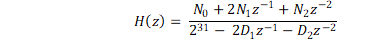
The device supports up to 12 programmable digital biquad filters. These highly efficient filters achieve the desired frequence response. In digital signal processing, a digital biquad filter is a second-order, recursive linear filter with two poles and two zeros. Equation 2 gives the transfer function of each biquad filter:
The frequency response for the biquad filter section with default coefficients is flat at a gain of 0 dB (all-pass filter). The host device can override the frequency response by programming the biquad coefficients to achieve the desired frequency response for a low-pass, high-pass, or any other desired frequency shaping. The programmable coefficients for the mixer operation are located in the Section 8.6.2.1 and Section 8.6.2.2 sections. If biquad filtering is required, then the host device must write these coefficients values before powering up any ADC channels for recording. These programmable coefficients are 32-bit, two’s complement numbers. As described in Table 8-16, these biquad filters can be allocated for each output channel based on the BIQUAD_CFG[1:0] register setting of P0_R108. By setting BIQUAD_CFG[1:0] to 2'b00, the biquad filtering for all record channels is disabled and the host device can choose this setting if no additional filtering is required for the system application. See the PCM6xx0-Q1 Programmable Biquad Filter Configuration and Applications application report for further details.
| PROGRAMMABLE BIQUAD FILTER | RECORD OUTPUT CHANNEL ALLOCATION USING P0_R108_D[6:5] REGISTER SETTING | ||
|---|---|---|---|
| BIQUAD_CFG[1:0] =
2'b01 (1 Biquad per Channel) |
BIQUAD_CFG[1:0] =
2'b10 (Default) (2 Biquads per Channel) |
BIQUAD_CFG[1:0] = 2'b11
(3 Biquads per Channel) |
|
| SUPPORTS ALL 8 CHANNELS | SUPPORTS UP TO 6 CHANNELS | SUPPORTS UP TO 4 CHANNELS | |
| Biquad filter 1 | Allocated to output channel 1 | Allocated to output channel 1 | Allocated to output channel 1 |
| Biquad filter 2 | Allocated to output channel 2 | Allocated to output channel 2 | Allocated to output channel 2 |
| Biquad filter 3 | Allocated to output channel 3 | Allocated to output channel 3 | Allocated to output channel 3 |
| Biquad filter 4 | Allocated to output channel 4 | Allocated to output channel 4 | Allocated to output channel 4 |
| Biquad filter 5 | Not used | Allocated to output channel 1 | Allocated to output channel 1 |
| Biquad filter 6 | Not used | Allocated to output channel 2 | Allocated to output channel 2 |
| Biquad filter 7 | Not used | Allocated to output channel 3 | Allocated to output channel 3 |
| Biquad filter 8 | Not used | Allocated to output channel 4 | Allocated to output channel 4 |
| Biquad filter 9 | Allocated to output channel 5 | Allocated to output channel 5 | Allocated to output channel 1 |
| Biquad filter 10 | Allocated to output channel 6 | Allocated to output channel 6 | Allocated to output channel 2 |
| Biquad filter 11 | Not used | Allocated to output channel 5 | Allocated to output channel 3 |
| Biquad filter 12 | Not used | Allocated to output channel 6 | Allocated to output channel 4 |
Table 8-17 shows the biquad filter coefficients mapping to the register space.
| PROGRAMMABLE BIQUAD FILTER | BIQUAD FILTER COEFFICIENTS REGISTER MAPPING | PROGRAMMABLE BIQUAD FILTER | BIQUAD FILTER COEFFICIENTS REGISTER MAPPING |
|---|---|---|---|
| Biquad filter 1 | P2_R8-R27 | Biquad filter 7 | P3_R8-R27 |
| Biquad filter 2 | P2_R28-R47 | Biquad filter 8 | P3_R28-R47 |
| Biquad filter 3 | P2_R48-R67 | Biquad filter 9 | P3_R48-R67 |
| Biquad filter 4 | P2_R68-R87 | Biquad filter 10 | P3_R68-R87 |
| Biquad filter 5 | P2_R88-R107 | Biquad filter 11 | P3_R88-R107 |
| Biquad filter 6 | P2_R108-R127 | Biquad filter 12 | P3_R108-R127 |