ZHCSIE3B June 2018 – May 2019 LMZM33606
PRODUCTION DATA.
- 1 特性
- 2 应用
- 3 说明
- 4 修订历史记录
- 5 Pin Configuration and Functions
- 6 Specifications
-
7 Detailed Description
- 7.1 Overview
- 7.2 Functional Block Diagram
- 7.3
Feature Description
- 7.3.1 Adjusting the Output Voltage
- 7.3.2 Input Capacitor Selection
- 7.3.3 Output Capacitor Selection
- 7.3.4 Transient Response
- 7.3.5 Feed-Forward Capacitor
- 7.3.6 Switching Frequency (RT)
- 7.3.7 Synchronization (SYNC/MODE)
- 7.3.8 Output Enable (EN)
- 7.3.9 Programmable System UVLO (EN)
- 7.3.10 Internal LDO and BIAS_SEL
- 7.3.11 Power Good (PGOOD) and Power Good Pull-Up (PGOOD_PU)
- 7.3.12 Mode Select (Auto or FPWM)
- 7.3.13 Soft Start and Voltage Tracking
- 7.3.14 Voltage Dropout
- 7.3.15 Overcurrent Protection (OCP)
- 7.3.16 Thermal Shutdown
- 7.4 Device Functional Modes
- 8 Application and Implementation
- 9 Power Supply Recommendations
- 10Layout
- 11器件和文档支持
- 12机械、封装和可订购信息
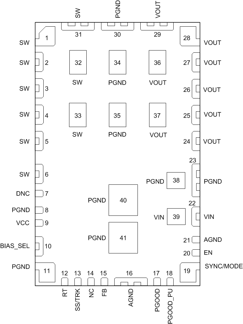
5 Pin Configuration and Functions
RLX Package
41-Pin QFN
Top View

Pin Functions
| PIN | TYPE | DESCRIPTION | |
|---|---|---|---|
| NAME | NO. | ||
| AGND | 16, 21 | G | Analog ground. Zero voltage reference for internal references and logic. These pins are not connected to one another internal to the device and must be connected to one another externally. Do not connect these pins to PGND; the AGND to PGND connection is made internal to the device. See the Layout section of the datasheet for a recommended layout. |
| BIAS_SEL | 10 | I | Optional BIAS LDO supply input. An internal 470 nF capacitor is placed between this pin and PGND. Do not float; tie to PGND if not used. Tie to VOUT if 3.3 V ≤ VOUT ≤ 18 V, or tie to an external 3.3-V or 5-V rail if available to improve efficiency. |
| DNC | 7 | — | Do not connect. This pin is connected to internal circuitry. Do not connect this pin to AGND, PGND, or any other voltage. This pin must be soldered to an isolated pad.. |
| EN | 20 | I | Precision enable input to regulator. Do not float. High = ON, Low = OFF. Can be tied to VIN. Precision enable input allows adjustable system UVLO using external resistor divider. |
| FB | 15 | I | Feedback input. Connect the center point of the feedback resistor divider to this pin. Connect the upper resistor (RFBT) of the feedback divider to VOUT at the desired point of regulation. Connect the lower resistor (RFBB) of the feedback divider to AGND. |
| NC | 14 | — | Not internally connected. |
| PGND | 8, 11, 23, 30, 34, 35, 38, 40, 41 | G | Power ground. This is the return current path for the power stage of the device. Connect these pins to the low side of the input source, load, and bypass capacitors associated with VIN and VOUT using power ground planes on the PCB. Not all pins are connected to PGND internal to the device; connections must be made externally. Connect pad 40 and 41 to the ground planes using multiple vias for good thermal performance. |
| PGOOD | 17 | O | Open drain output for power-good flag. Internal to the device, a 100-kΩ pullup resistor is placed between this pin and the PGOOD_PU pin. |
| PGOOD_PU | 18 | I | Power-good pull-up supply. Connect to logic rail or other DC voltage no higher than 20 V. |
| RT | 12 | I | An external timing resistor connected between this pin and AGND adjusts the switching frequency of the device. If floating, the default switching frequency is 500 kHz. Do not short to ground. |
| SS/TRK | 13 | I | Soft start / tracking control pin. Leave this pin floating to use the 5-ms internal soft-start ramp.To increase the internal soft start ramp time, simply connect a capacitor between this pin and AGND. This pin sources 2-μA of current to charge this external capacitor. Connect to external voltage ramp for tracking. Do not connect to ground. |
| SW | 1, 2, 3, 4, 5, 6, 31, 32, 33 | O | Switch node. Connect these pins to a small copper island under the device for thermal relief. Do not place any external components on these pins or tie them to a pin of another function. |
| SYNC/MODE | 19 | I | Synchronization input and Mode setting pin. Do not float; tie to AGND or logic high if not used. Connect to an external clock to synchronize (see Synchronization (SYNC/MODE)). Connect to AGND to select Auto mode or connect to logic high to select FPWM mode. (see Mode Select (Auto or FPWM)). |
| VCC | 9 | O | Output of internal bias supply. Used to supply internal control circuits and drivers. Do not place any external component on this pin or tie it to a pin of another function. |
| VIN | 22, 39 | I | Input supply voltage. Connect external input capacitors between these pins and PGND. |
| VOUT | 24, 25, 26, 27, 28, 29, 36, 37 | O | Output voltage. These pins are connected to the output of the internal inductor. Connect these pins to the output VOUT load and connect external bypass capacitors between these pins and PGND. |