ZHCSIE3B June   2018  – May 2019 LMZM33606

PRODUCTION DATA.  

  1. 特性
  2. 应用
    1.     简化电路原理图
  3. 说明
    1.     最小解决方案尺寸
    2.     典型效率(自动模式)
  4. 修订历史记录
  5. Pin Configuration and Functions
    1.     Pin Functions
  6. Specifications
    1. 6.1 Absolute Maximum Ratings
    2. 6.2 ESD Ratings
    3. 6.3 Recommended Operating Conditions
    4. 6.4 Thermal Information
    5. 6.5 Electrical Characteristics
    6. 6.6 Switching Characteristics
    7. 6.7 Typical Characteristics (VIN = 12 V)
    8. 6.8 Typical Characteristics (VIN = 24 V)
    9. 6.9 Typical Characteristics (VIN = 36 V)
  7. Detailed Description
    1. 7.1 Overview
    2. 7.2 Functional Block Diagram
    3. 7.3 Feature Description
      1. 7.3.1  Adjusting the Output Voltage
      2. 7.3.2  Input Capacitor Selection
      3. 7.3.3  Output Capacitor Selection
      4. 7.3.4  Transient Response
      5. 7.3.5  Feed-Forward Capacitor
      6. 7.3.6  Switching Frequency (RT)
      7. 7.3.7  Synchronization (SYNC/MODE)
      8. 7.3.8  Output Enable (EN)
      9. 7.3.9  Programmable System UVLO (EN)
      10. 7.3.10 Internal LDO and BIAS_SEL
      11. 7.3.11 Power Good (PGOOD) and Power Good Pull-Up (PGOOD_PU)
      12. 7.3.12 Mode Select (Auto or FPWM)
      13. 7.3.13 Soft Start and Voltage Tracking
      14. 7.3.14 Voltage Dropout
      15. 7.3.15 Overcurrent Protection (OCP)
      16. 7.3.16 Thermal Shutdown
    4. 7.4 Device Functional Modes
      1. 7.4.1 Active Mode
      2. 7.4.2 Auto Mode
      3. 7.4.3 FPWM Mode
      4. 7.4.4 Shutdown Mode
  8. Application and Implementation
    1. 8.1 Application Information
    2. 8.2 Typical Application
      1. 8.2.1 Design Requirements
      2. 8.2.2 Detailed Design Procedure
        1. 8.2.2.1 Output Voltage Setpoint
        2. 8.2.2.2 Setting the Switching Frequency
        3. 8.2.2.3 Input Capacitors
        4. 8.2.2.4 Output Capacitor Selection
        5. 8.2.2.5 Feed-Forward Capacitor (CFF)
        6. 8.2.2.6 Application Curves
  9. Power Supply Recommendations
  10. 10Layout
    1. 10.1 Layout Guidelines
    2. 10.2 Layout Example
    3. 10.3 Theta JA vs PCB Area
    4. 10.4 Package Specifications
    5. 10.5 EMI
      1. 10.5.1 EMI Plots
  11. 11器件和文档支持
    1. 11.1 器件支持
      1. 11.1.1 第三方产品免责声明
    2. 11.2 接收文档更新通知
    3. 11.3 社区资源
    4. 11.4 商标
    5. 11.5 静电放电警告
    6. 11.6 Glossary
  12. 12机械、封装和可订购信息
    1. 12.1 Tape and Reel Information

封装选项

请参考 PDF 数据表获取器件具体的封装图。

机械数据 (封装 | 引脚)
  • RLX|41
散热焊盘机械数据 (封装 | 引脚)
订购信息

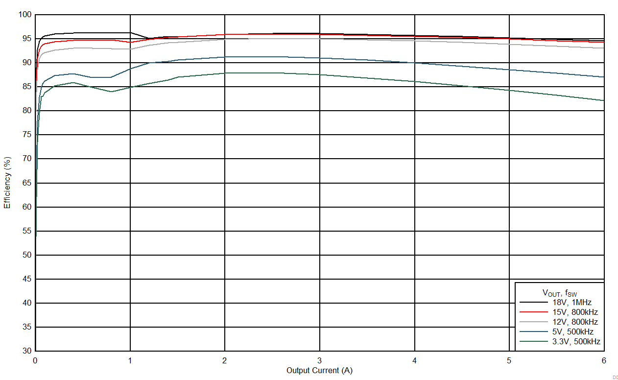
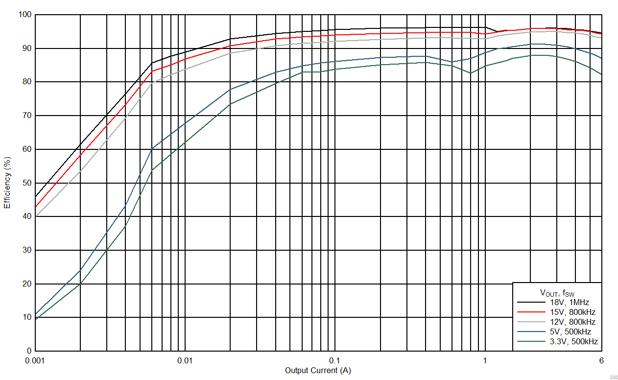
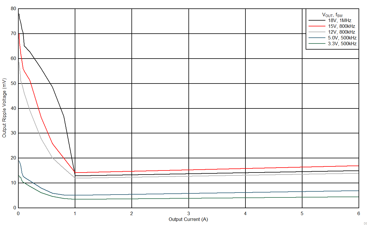
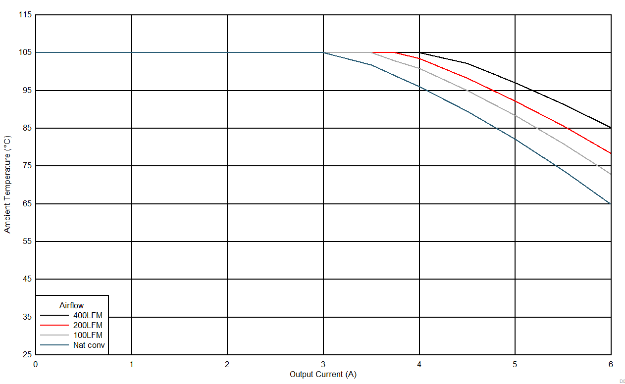
Typical Characteristics (VIN = 24 V)

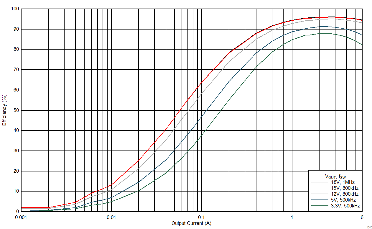
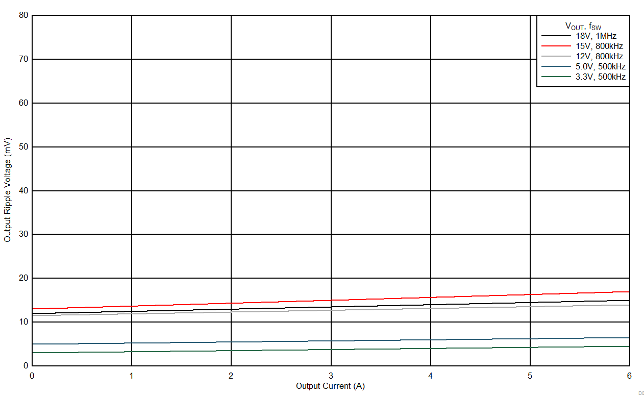
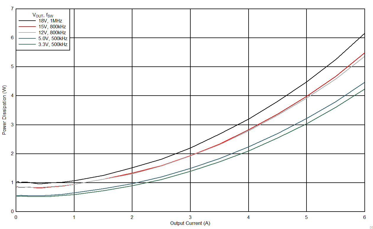
The typical characteristic data has been developed from actual products tested at 25°C. This data is considered typical for the device.
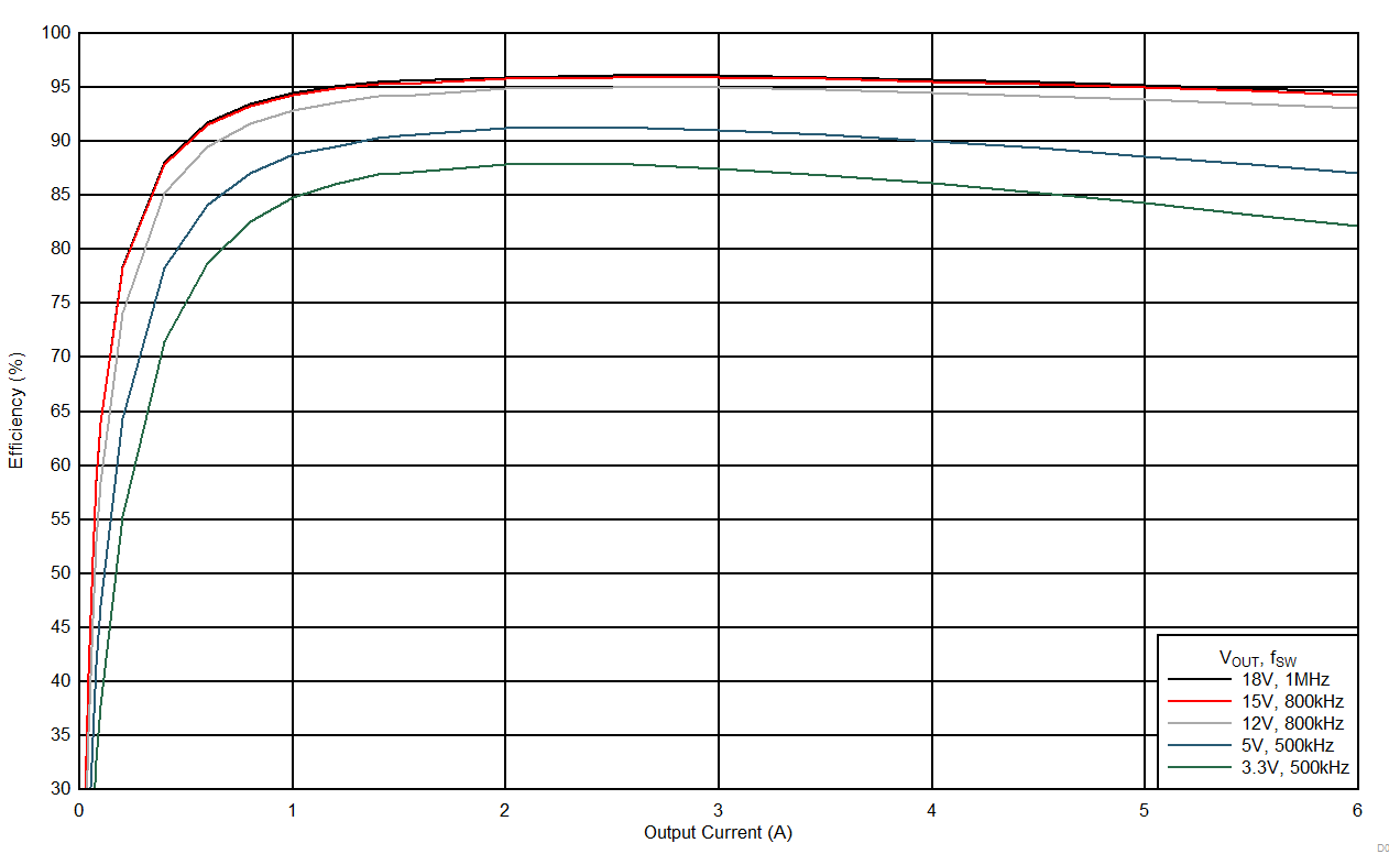
LMZM33606 D004_24VeffPWMLin2.gif
FPWM Mode Linear Scale
Figure 11. Efficiency vs Output Current
LMZM33606 D005_24VeffPWMLog.gif
FPWM Mode Log Scale
Figure 13. Efficiency vs Output Current
LMZM33606 D007_24VRippleFPWM1.gif
FPWM Mode COUT = 4 × 47 µF ceramic
Figure 15. Output Voltage Ripple
LMZM33606 D008_24VPdis.gif
Figure 17. Power Dissipation
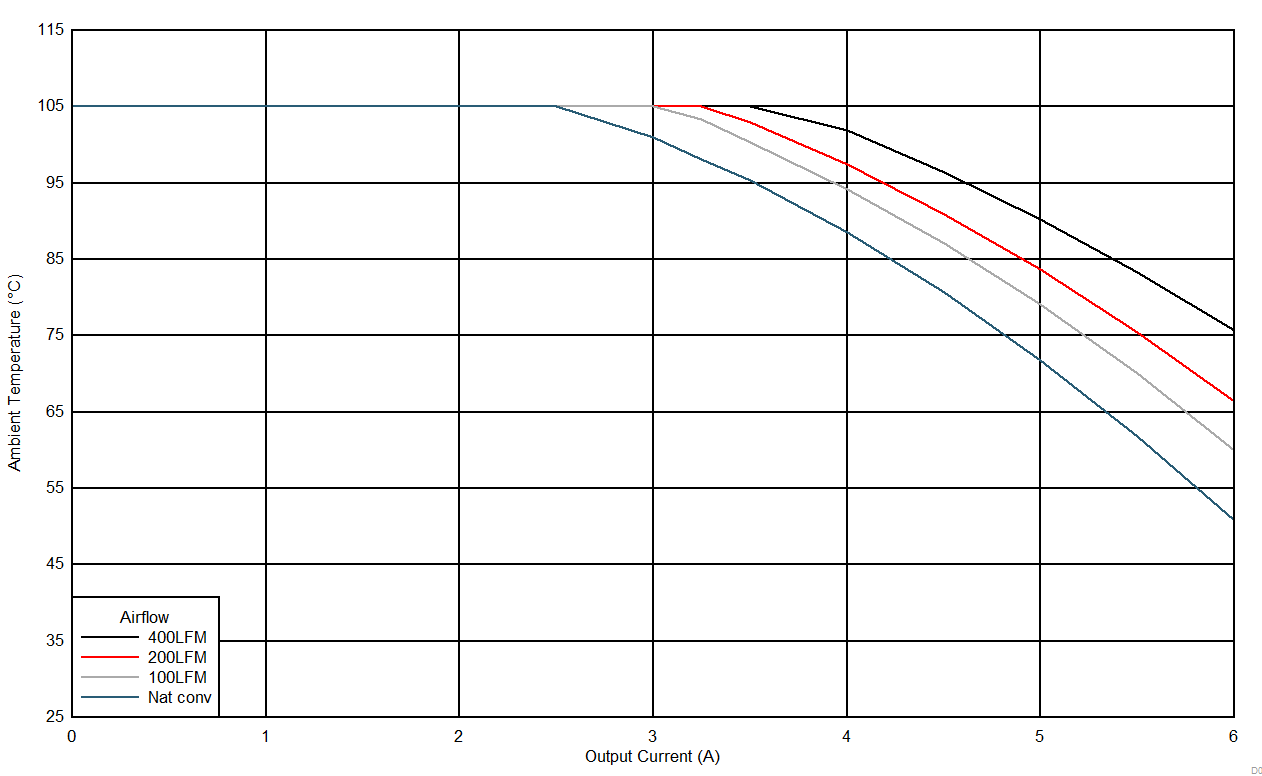
LMZM33606 D010_24Vto5VSOA.gif
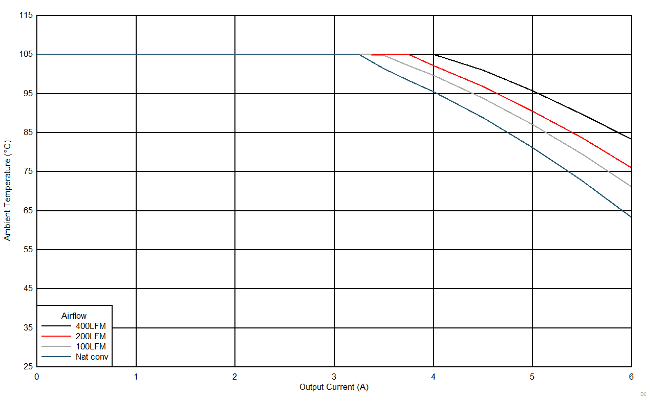
VOUT = 5 V fSW = 500 kHz
PCB = 75 mm × 75 mm, 4-layer, 2 oz. copper
Figure 19. Safe Operating Area
LMZM33606 D002_24VeffAutoLin2.gif
Auto Mode Linear Scale
Figure 12. Efficiency vs Output Current
LMZM33606 D003_24VeffAutoLog.gif
Auto Mode Log Scale
Figure 14. Efficiency vs Output Current
LMZM33606 D006_24VRippleAuto.gif
Auto Mode COUT = 4 × 47 µF ceramic
Figure 16. Output Voltage Ripple
LMZM33606 D011_24Vto33VSOA.gif
VOUT = 3.3 V fSW = 500 kHz
PCB = 75 mm × 75 mm, 4-layer, 2 oz. copper
Figure 18. Safe Operating Area
LMZM33606 D009_24Vto12VSOA.gif
VOUT = 12 V fSW = 800 kHz
PCB = 75 mm × 75 mm, 4-layer, 2 oz. copper
Figure 20. Safe Operating Area