ZHCSIE3B June 2018 – May 2019 LMZM33606
PRODUCTION DATA.
- 1 特性
- 2 应用
- 3 说明
- 4 修订历史记录
- 5 Pin Configuration and Functions
- 6 Specifications
-
7 Detailed Description
- 7.1 Overview
- 7.2 Functional Block Diagram
- 7.3
Feature Description
- 7.3.1 Adjusting the Output Voltage
- 7.3.2 Input Capacitor Selection
- 7.3.3 Output Capacitor Selection
- 7.3.4 Transient Response
- 7.3.5 Feed-Forward Capacitor
- 7.3.6 Switching Frequency (RT)
- 7.3.7 Synchronization (SYNC/MODE)
- 7.3.8 Output Enable (EN)
- 7.3.9 Programmable System UVLO (EN)
- 7.3.10 Internal LDO and BIAS_SEL
- 7.3.11 Power Good (PGOOD) and Power Good Pull-Up (PGOOD_PU)
- 7.3.12 Mode Select (Auto or FPWM)
- 7.3.13 Soft Start and Voltage Tracking
- 7.3.14 Voltage Dropout
- 7.3.15 Overcurrent Protection (OCP)
- 7.3.16 Thermal Shutdown
- 7.4 Device Functional Modes
- 8 Application and Implementation
- 9 Power Supply Recommendations
- 10Layout
- 11器件和文档支持
- 12机械、封装和可订购信息
7.3.13 Soft Start and Voltage Tracking
The soft-start and tracking features control the output voltage ramp during start-up. The soft-start feature reduces inrush current during start-up and improves system performance and reliability. If the SS/TRK pin is floating, the LMZM33606 starts up following the fixed, 5-ms internal soft-start ramp. Use CSS to extend soft-start time when there are a large amount of output capacitors, or the output voltage is high, or the output is heavily loaded during start-up.
If longer soft-start time is desired, an external capacitor can be added from SS/TRK pin to AGND. There is a 2 µA (typical) internal current source, ISSC, to charge the external capacitor. For a desired soft-start time tSS, capacitance of CSS can be found by Equation 6.
where
- CSS = soft-start capacitor value (F)
- ISSC = soft-start charging current (A)
- tSS = desired soft-start time(s)
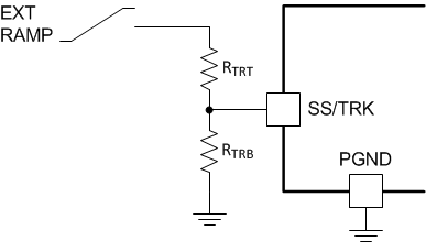
LMZM33606 can track an external voltage ramp applied to the SS/TRK pin, if the ramp is slower than the internal soft-start ramp. The external ramp final voltage after start-up must be greater than 1.5 V to avoid noise interfering with the reference voltage. Figure 40 shows how to use resistor divider to set VOUT to follow an external ramp.
 Figure 40. Soft-Start Tracking External Ramp